

Preparation method of germanium-base schottky transistor
A technology of transistors and MOS transistors, which is applied in the field of Ge-based Schottky preparation, can solve problems such as difficulty in realizing shallow junctions, large off-state leakage current, and small on-state drive current, so as to improve morphology, reduce voids, The effect of improving performance
- Summary
- Abstract
- Description
- Claims
- Application Information
AI Technical Summary
Problems solved by technology
Method used
Image


Examples
Embodiment Construction
[0031] Below in conjunction with accompanying drawing and specific embodiment the present invention is described in further detail:
[0032] FIG. 1 is a flow chart of a method for fabricating NiGe schottky source and drain according to a preferred embodiment of the present invention. The method for making germanium-based Schottky transistor of the present invention comprises the following steps:
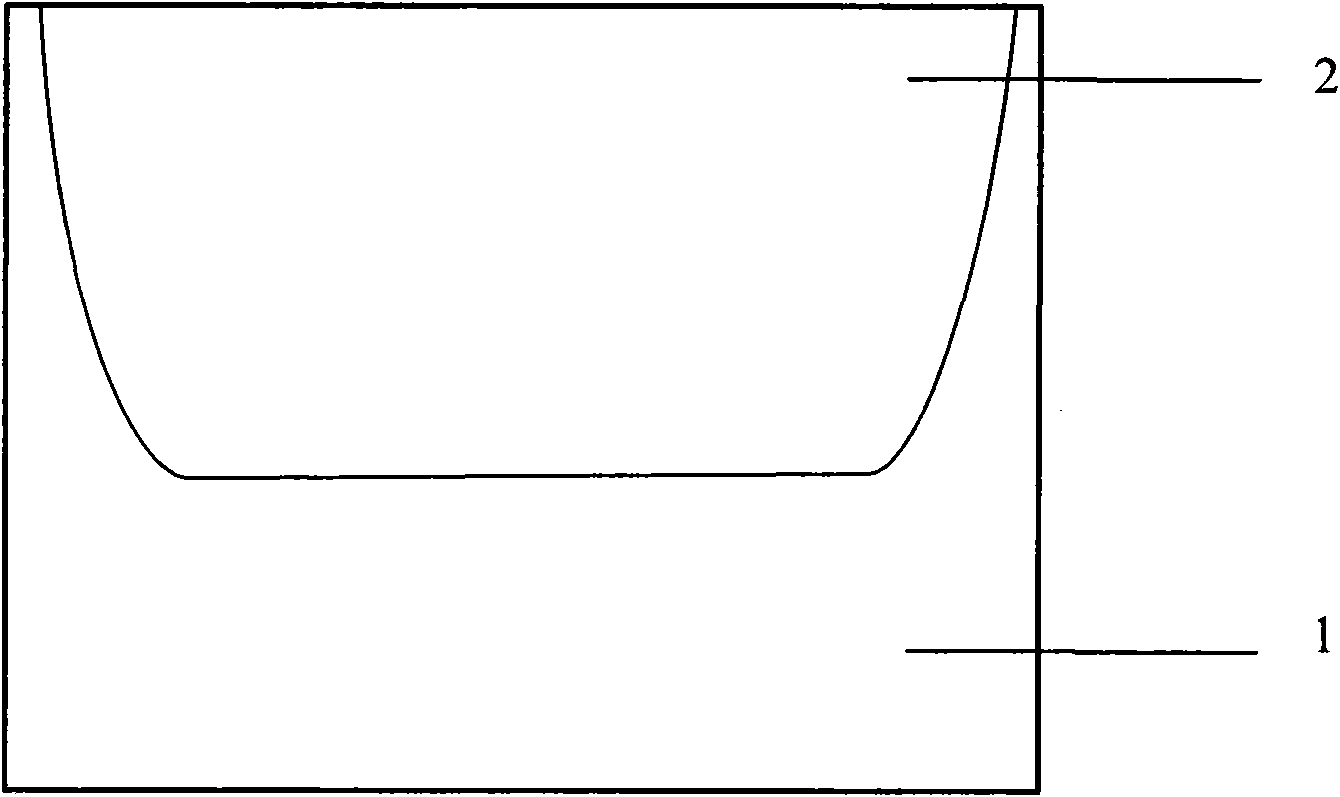
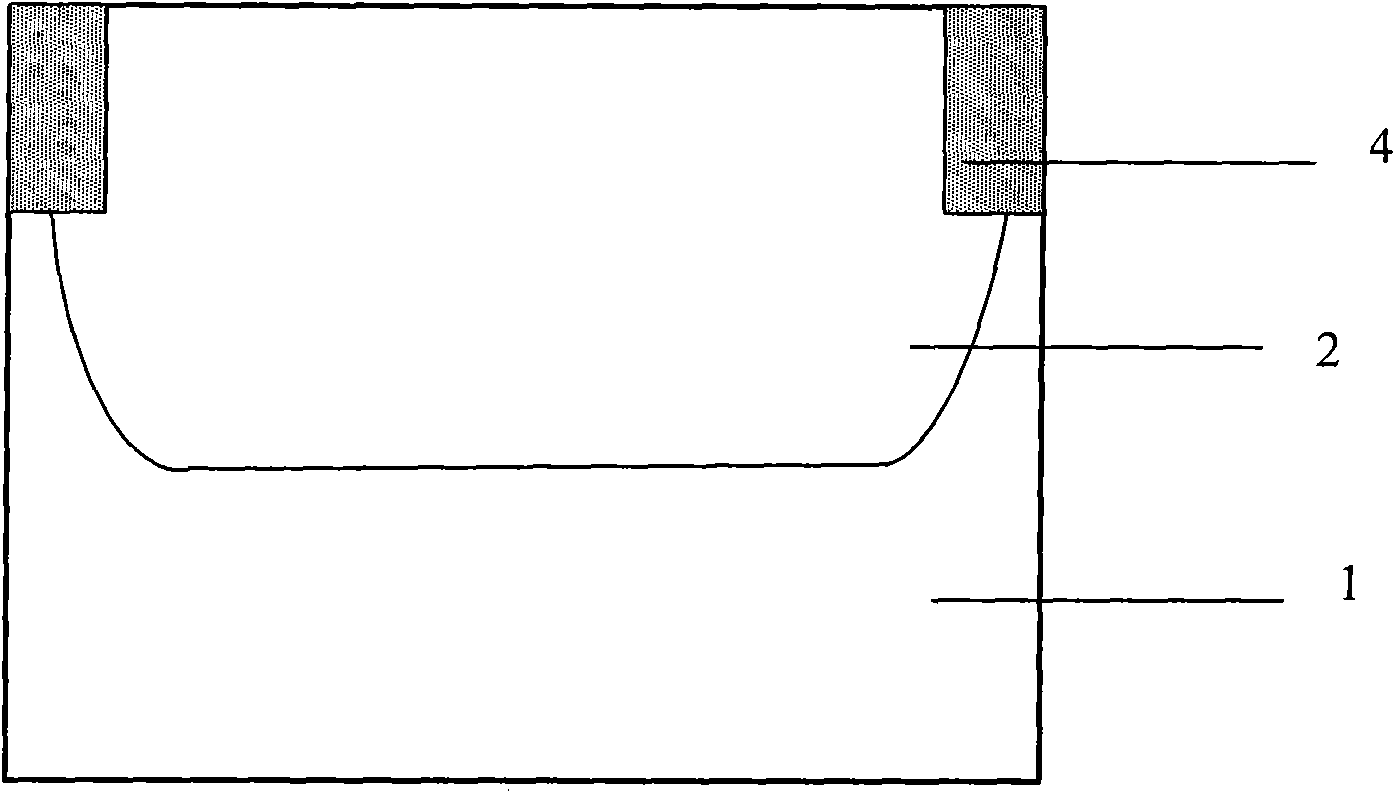
[0033] Step 1: Provide a germanium-based substrate. As shown in FIG. 1( a ), a semiconductor germanium substrate 1 is doped with P-type impurity Ga, wherein the semiconductor germanium substrate 1 can be a bulk germanium substrate or a germanium-on-insulator (GOI) substrate or the like.
[0034] Step 2: Fabricate the N-well region. Deposit a silicon oxide layer and a silicon nitride layer on the germanium substrate, define the N well region by photolithography, reactive ion etch away the silicon nitride in the N well region, and ion implant N-type impurities, such as phosphorus, an...
PUM
 Abstract
Description
Claims
Application Information