Charge pump circuit

A charge pump and circuit technology, applied in electrical components, static memory, instruments, etc., can solve problems such as residual charge misoperation, component capacitance component degradation of charge pump circuits, etc., and achieve the effect of solving component degradation or misoperation

Inactive Publication Date: 2008-05-07
SANYO ELECTRIC CO LTD +1
View PDF1 Cites 20 Cited by
  • Summary
  • Abstract
  • Description
  • Claims
  • Application Information

AI Technical Summary

Problems solved by technology

[0013] The main object of the present invention is to provide a charge pump circuit capable of solving the problems of deterioration of components (capacitance elements or charge transfer elements) constituting the charge pump circuit due to residual charges and malfunctions caused by residual charges.

Method used


Image

  • Charge pump circuit
  • Charge pump circuit
  • Charge pump circuit

Examples


Embodiment Construction

[0022] Next, embodiments of the present invention will be described with reference to the drawings.

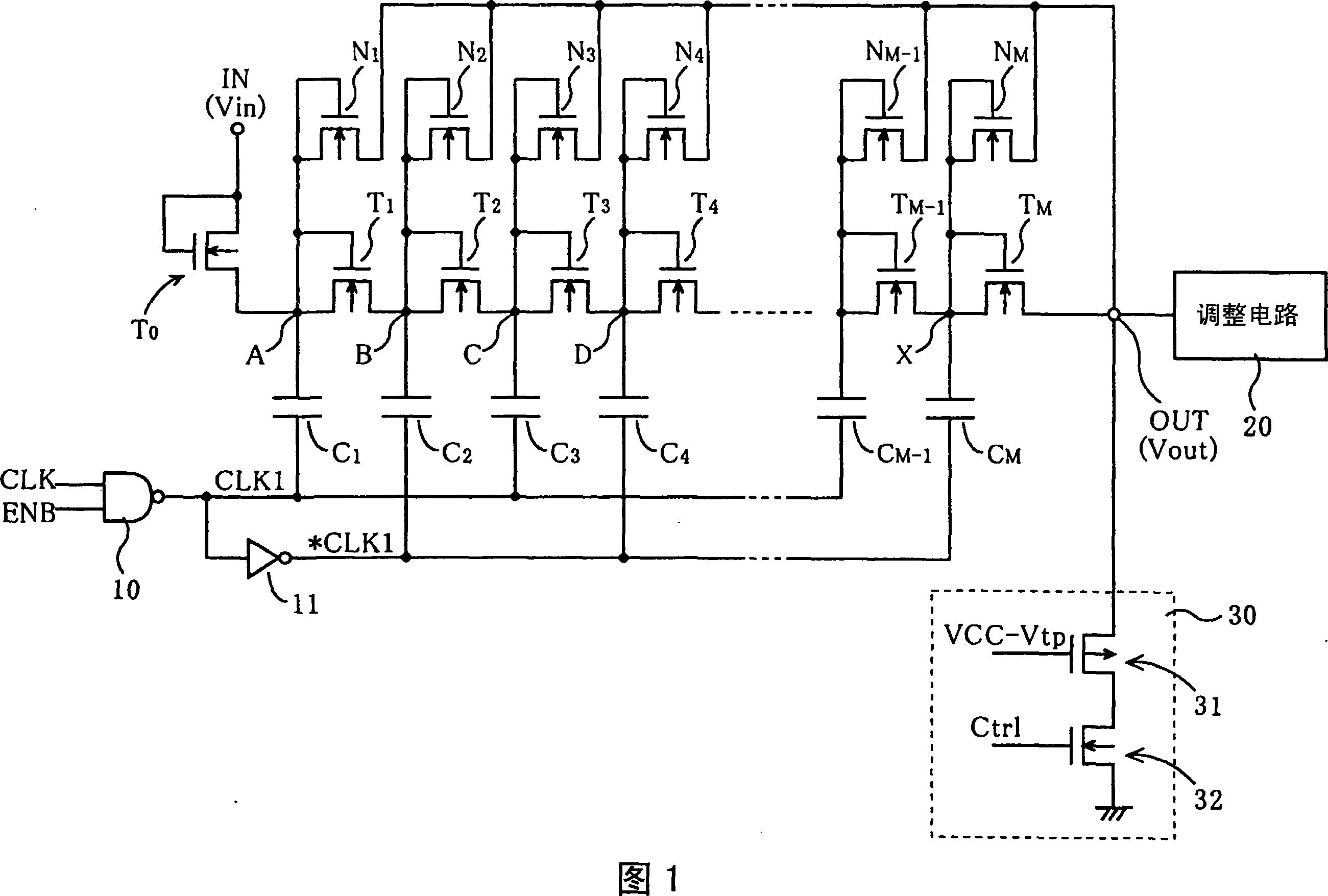
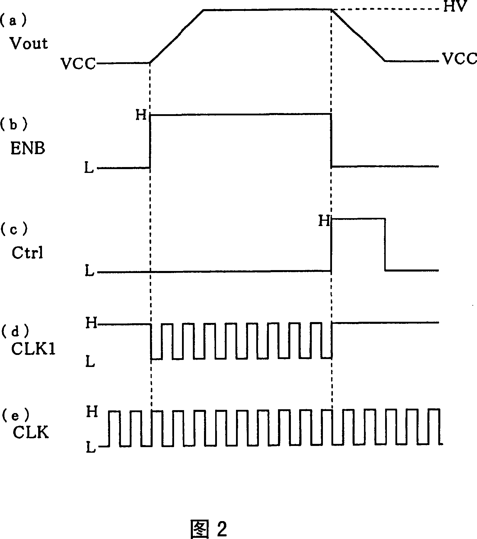
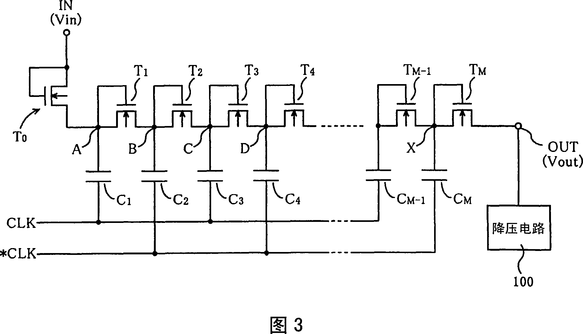
[0023] The charge pump circuit according to this embodiment boosts an input voltage Vin=VCC (for example, 3 volts) input to an input terminal IN, and outputs a high voltage HV (for example, approximately 20 volts) from an output terminal OUT as an output voltage Vout. As shown in FIG. 1, between the input terminal IN and the output terminal OUT, N-channel charge transfer MOS transistors To to T with the gate and drain short-circuited are connected in series. M (M is an arbitrary value). Each charge transfer MOS transistor To~T M The connection points of are set to nodes A to X.

[0024] Nodes A to X and capacitive element C 1 ~C M One terminal connection. That is, a plurality of block units composed of charge transfer MOS transistors and capacitive elements are connected in series. Capacitive element C 1 ~C M The other terminal is applied with the first clock signal CL...


PUM


Abstract

The invention is aimed at solving the problem of the deterioration happened to the elements (capacitance of a charge pump or a charge transferring unit) of a charge pump circuit as a result of the remaining charge and the problem of the faulty action caused by the remaining charge. An N channel type charge transferring MOS transistor (To-TM) which short-circuits a grid electrode and a drain electrode is serially connected between an input terminal (IN) and an output terminal (OUT). Joint points (joint A to X) of the charge transferring MOS transistor are connected with a terminal of a capacitance unit (C1 to CM H02M 3 / 07 3 6 1 2007 / 10 / 26 101174789 2008 / 5 / 7 000000000 Sanyo Electric Co. Japan Raijun Toju Kichikawa Sadao lixiang lan 11021 The Patent Agency of the Chinese Academy of Sciences Inside the Chinese Academy of Sciences, No.52 Sanlihe Road, Fuwai, Beijing 100864 Japan 2006 / 10 / 31 2006-295100

Description

technical field [0001] The present invention relates to a charge pump circuit (Charge Pump Circuit) that generates high voltage from low voltage, in particular to a charge pump circuit with a step-down circuit. Background technique [0002] For example, in nonvolatile semiconductor memory devices such as EEPROM (Electrically Programmable Read Only Memory), it is necessary to supply a positive high voltage (or a negative high voltage) higher than a power supply voltage to the memory cells. In such a situation where a high voltage is required, a method of building a charge pump circuit into a device is widely used. [0003] FIG. 3 is a circuit diagram of a charge pump circuit according to a conventional example. This charge pump circuit boosts an input voltage Vin (=VCC) input to an input terminal IN, and outputs a high voltage HV from an output terminal OUT as an output voltage Vout. Between the input terminal IN and the output terminal OUT, N-channel charge transfer MOS tr...

Claims


Application Information

Patent Timeline
Patent Type & Authority Applications(China)
IPC IPC(8): H02M3/07
CPCH02M3/073G11C5/145
Inventor 赖俊树吉川定男
Owner SANYO ELECTRIC CO LTD
Why Eureka
Try Eureka