Low frequency analog circuit design method and its low frequency analog circuit
一种模拟电路、设计方法的技术,应用在低频放大器、带有半导体器件/放电管的放大器、电气元件等方向,能够解决违背等问题
- Summary
- Abstract
- Description
- Claims
- Application Information
AI Technical Summary
Problems solved by technology
Method used
Image

Examples
Embodiment Construction
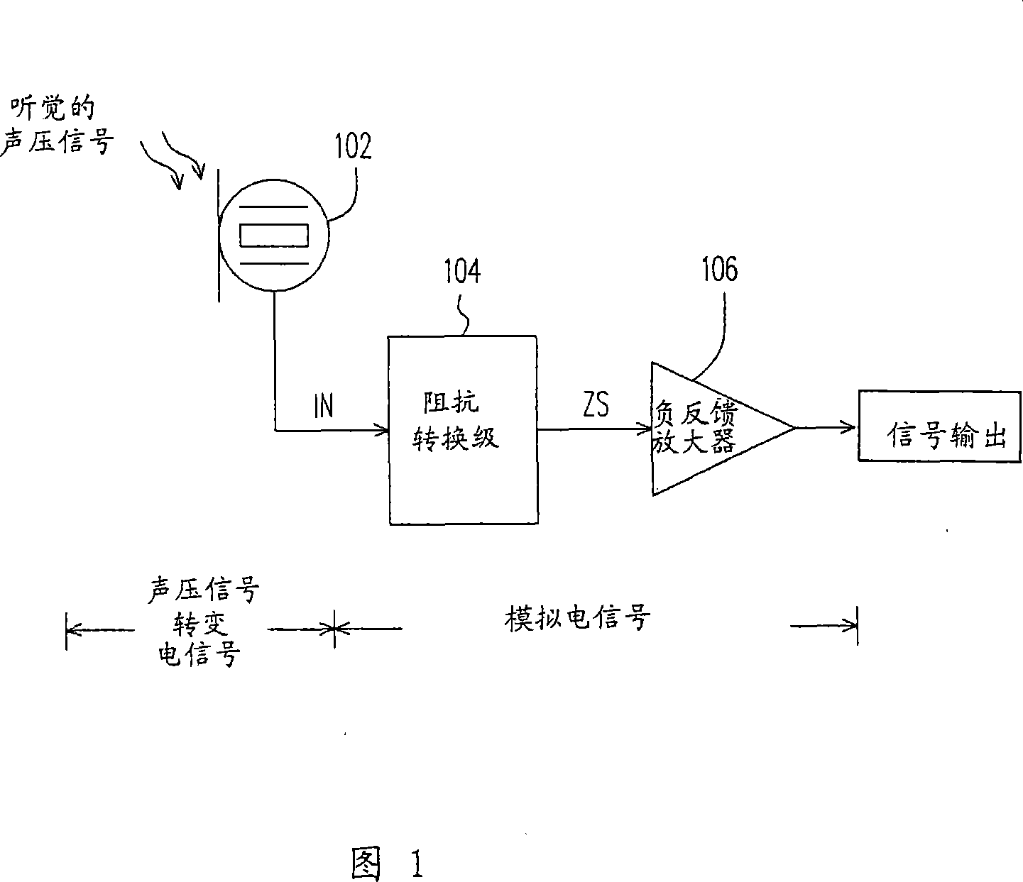
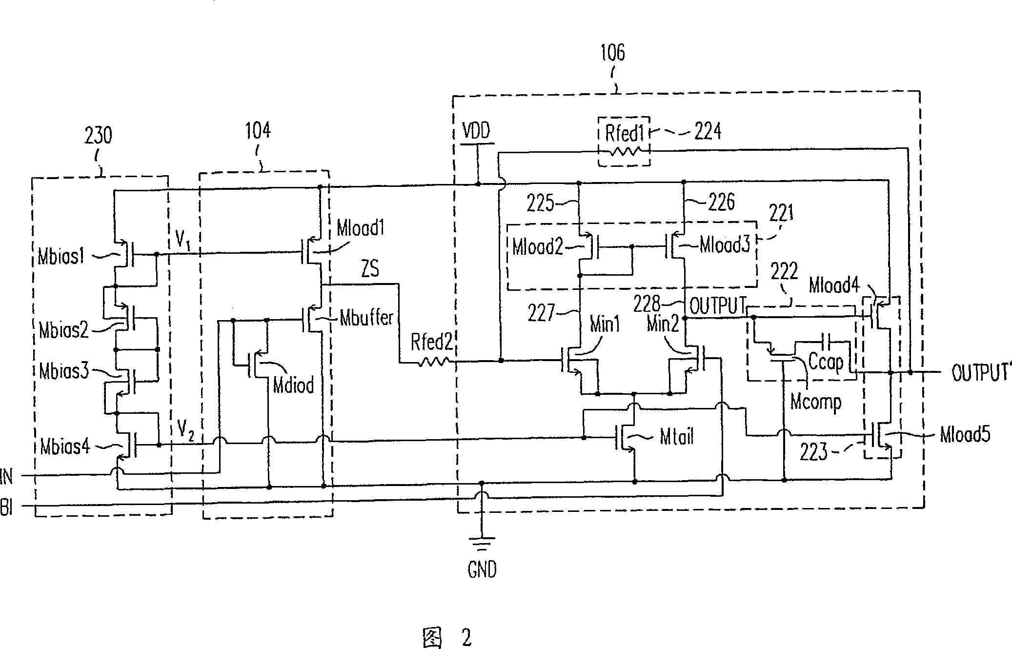
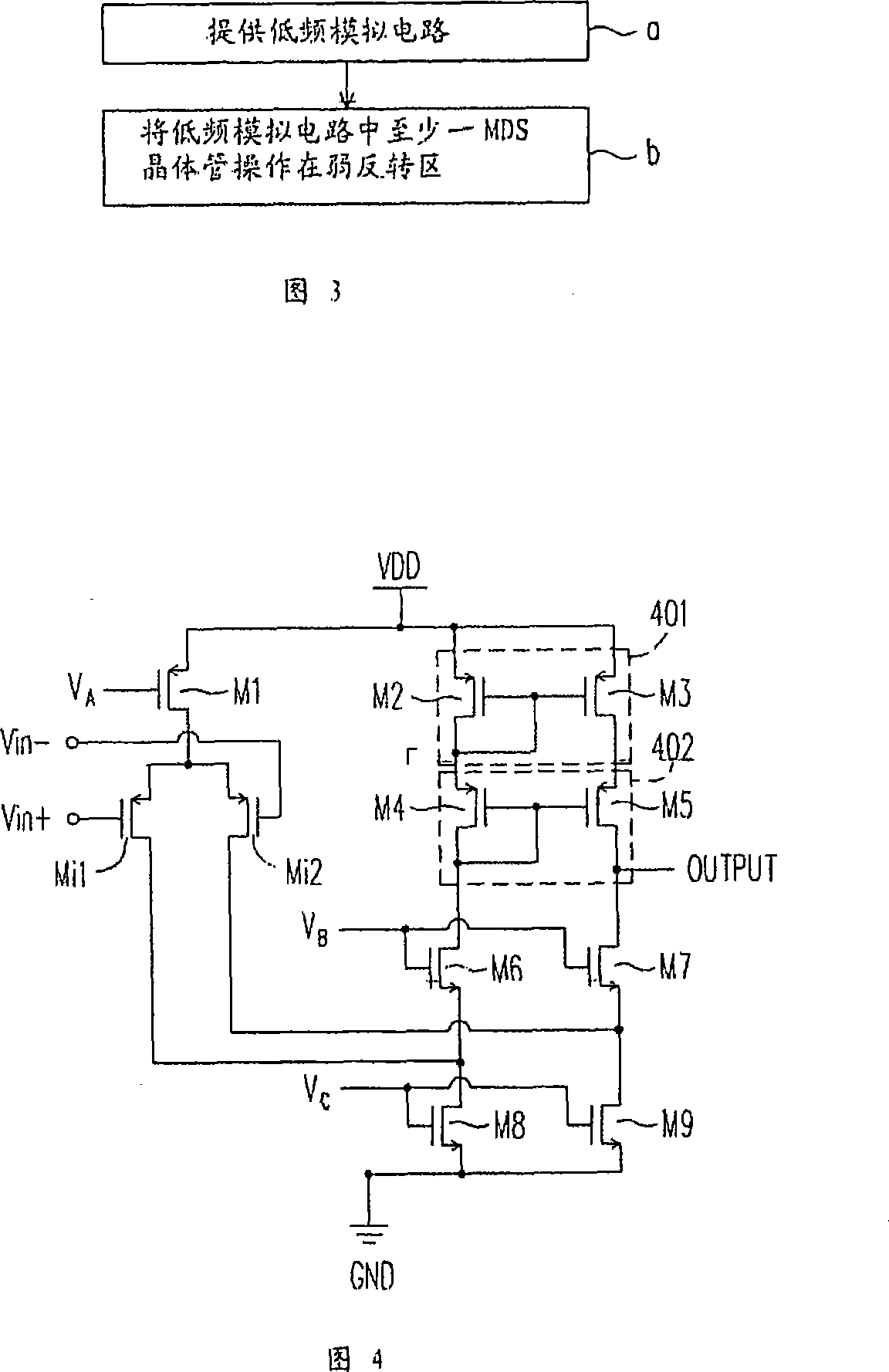
[0047] For convenience, the following description will use NMOS for illustration, but it is not intended to limit the scope of the present invention.
[0048] If the NMOS transistor is operated at V gs -V th Under the condition of gs -V th Under the condition of D It can be represented by the following formula (4):
[0049] I D = I D 0 ( W / L ) e ( V gs / nVt ) . . . . . . ( 4 )
[0050] Where W and L represent the width and length of the MOS transistor respectively, and n=(C js +C ox ) / C ox , C ox Indicates...
PUM
 Abstract
Description
Claims
Application Information
 - R&D
- Intellectual Property
- Life Sciences
- Materials
- Tech Scout
- Unparalleled Data Quality
- Higher Quality Content
- 60% Fewer Hallucinations
Browse by: Latest US Patents, China's latest patents, Technical Efficacy Thesaurus, Application Domain, Technology Topic, Popular Technical Reports.
© 2025 PatSnap. All rights reserved.Legal|Privacy policy|Modern Slavery Act Transparency Statement|Sitemap|About US| Contact US: help@patsnap.com