Supercharge Your Innovation With Domain-Expert AI Agents!

Circuit-design supporting apparatus, circuit-design supporting method, computer product, and printed-circuit-board manufacturing method

一种电路设计、支持装置的技术,应用在CAD电路设计、计算机辅助设计、电路等方向,能够解决增加电路设计者工作量等问题

Inactive Publication Date: 2008-06-11
FUJITSU LTD
View PDF1 Cites 4 Cited by
  • Summary
  • Abstract
  • Description
  • Claims
  • Application Information

AI Technical Summary

Problems solved by technology

Therefore, the workload of the circuit designer is increased

Method used


Image

  • Circuit-design supporting apparatus, circuit-design supporting method, computer product, and printed-circuit-board manufacturing method
  • Circuit-design supporting apparatus, circuit-design supporting method, computer product, and printed-circuit-board manufacturing method
  • Circuit-design supporting apparatus, circuit-design supporting method, computer product, and printed-circuit-board manufacturing method

Examples


Embodiment Construction

[0037] Exemplary embodiments according to the present invention will be described in detail below with reference to the accompanying drawings. Incidentally, in these embodiments, cases where the present invention is applied to FPGAs are mainly described.

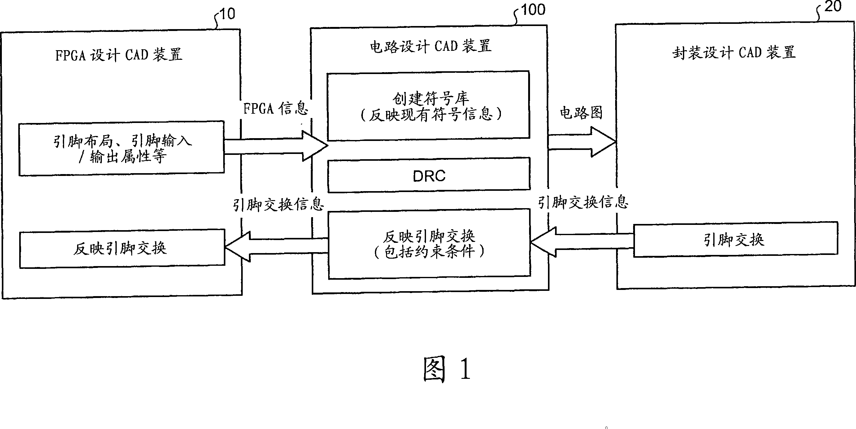
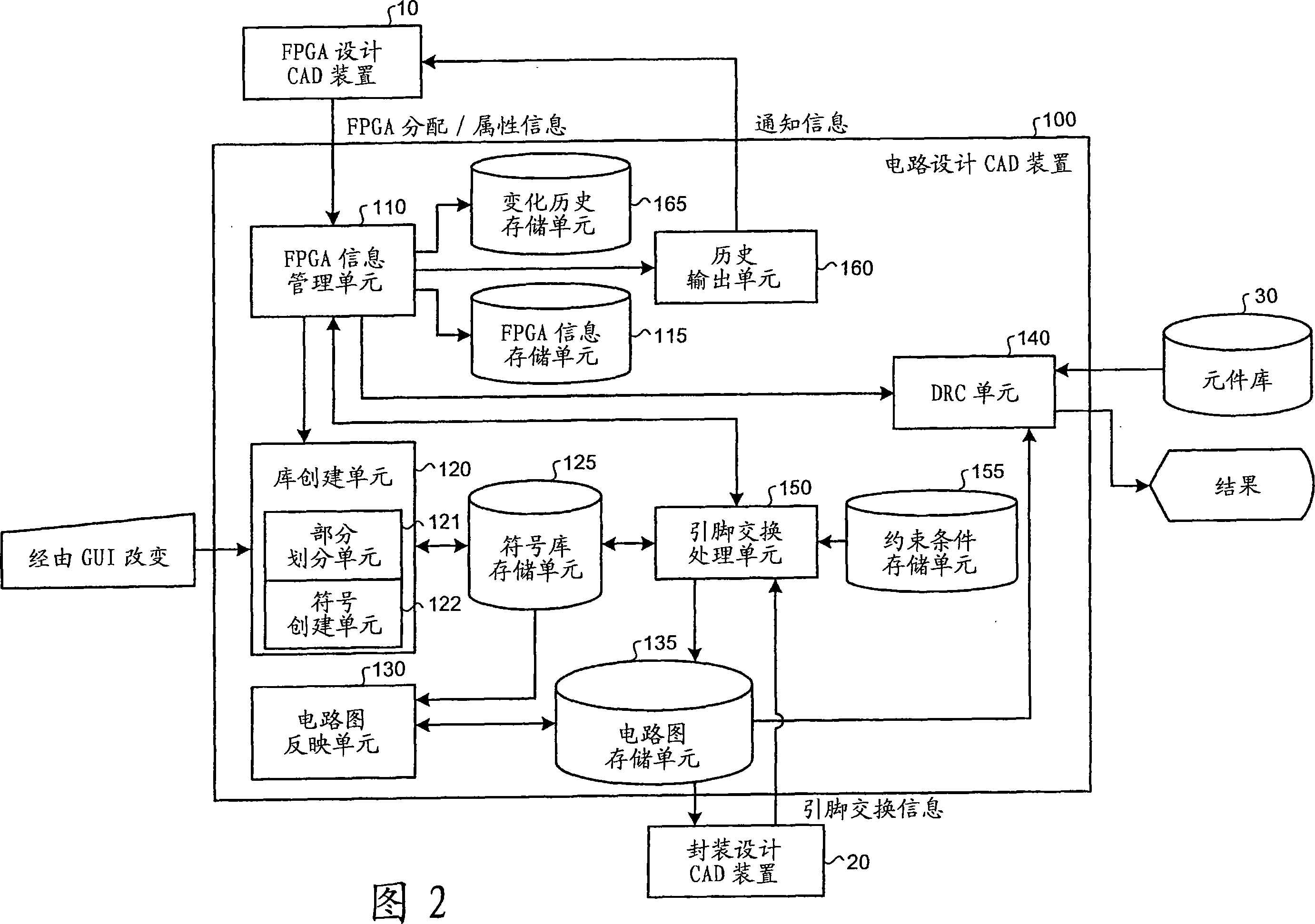
[0038] First, the principle of FPGA co-design according to the first embodiment of the present invention will be described. FIG. 1 is an explanatory diagram for explaining the principle of FPGA co-design according to the first embodiment. As shown in the figure, in the FPGA collaborative design according to the first embodiment, including: an FPGA design CAD device 10 supporting FPGA design; a package design CAD device 20 supporting a package design of a printed circuit board; and a circuit design CAD device 100 , which serves as a circuit design support device that supports circuit designs coordinated with each other to support a designer.

[0039] Specifically, the circuit design CAD apparatus 100 receives FPGA informati...


PUM


Abstract

The invention provides a circuit design support device and method, a computer product and a method for manufacturing a printed circuit board. The FPGA information management unit acquires FPGA information such as pin assignment information and attribute information created by the FPGA design CAD device. The library creating unit uses the FPGA information to create a symbol library. The pin swap processing unit acquires pin swap information from the package design CAD device, and reflects the pin swap in symbol libraries, FPGA information, circuit diagrams, and constraint conditions. The change history of the FPGA information is stored in the change history storage unit. The history output unit outputs information for notifying the FPGA design CAD device (10) of the pin swap based on the change history stored in the change history storage unit.

Description

technical field [0001] The present invention relates to a technique for supporting (assisting) in designing a circuit in which a programmable logic device (PLD) is used as an element. Background technique [0002] When designing a circuit in which a PLD such as an FPGA (Field Programmable Gate Array) is used as an element, the pin assignment of the PLD in the element design can be changed in the package design. This is because, in the PLD, the motion inside the element can be changed by rewriting the program, so that the pins of the PLD can be replaced at the package design stage to easily perform the pin layout. [0003] When the pin assignment is changed in the package design, it is necessary to reflect the change of the pin assignment in the package design in the PLD design information, so as to ensure the consistency of the package design information and the PLD design information. Therefore, a technique of reflecting pin replacement in package design in PLD design info...

Claims


Application Information

Patent Timeline
Patent Type & Authority Applications(China)
IPC IPC(8): G06F17/50
CPCG06F17/5054G06F30/34H01L21/00
Inventor 加藤嘉之青山久志
Owner FUJITSU LTD
Features
  • R&D
  • Intellectual Property
  • Life Sciences
  • Materials
  • Tech Scout
  • Unparalleled Data Quality
  • Higher Quality Content
  • 60% Fewer Hallucinations
Learn More