Writing circuit and method for flash memory
A technology for writing circuits and flash memory, applied in information storage, static memory, adjusting electrical variables, etc., can solve the problems of high difficulty in circuit implementation, decreased accuracy, and large chip area, shortening writing time, and reducing design complexity. degree and effect
- Summary
- Abstract
- Description
- Claims
- Application Information
AI Technical Summary
Problems solved by technology
Method used
Image
Examples
Embodiment Construction
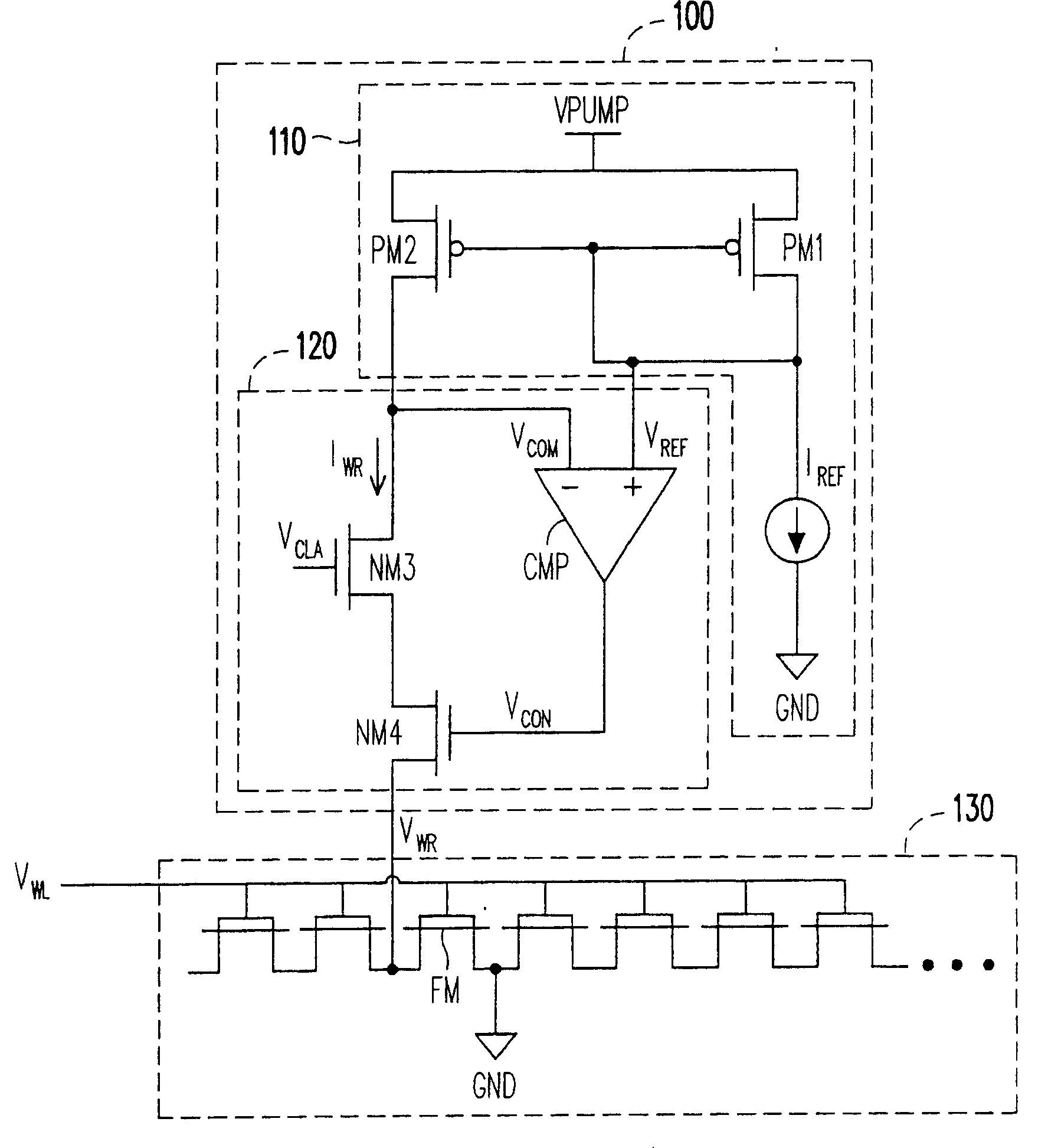
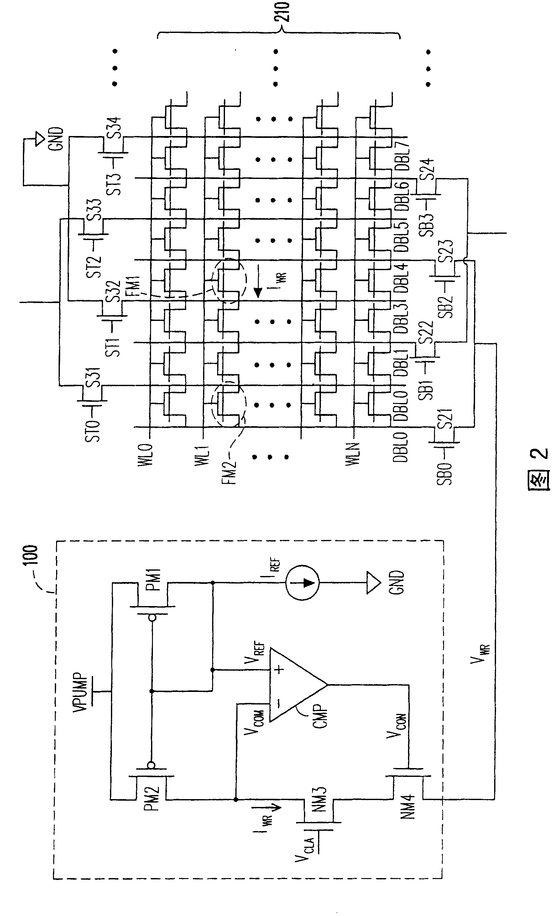
[0019] figure 1 It is a circuit diagram of a writing circuit of a flash memory according to an embodiment of the present invention. The writing circuit 100 includes a writing unit 110 and a detecting unit 120 , and the writing unit 100 is used to perform a writing operation on the storage element FM in the storage unit 130 . In this embodiment, the storage element FM is a floating gate memory, that is, a type of flash memory. The control gate of the storage element FM is coupled to a word line, and the word line can apply a word line voltage V to the control terminal (control gate) of the storage element FM. WL .
[0020] The write circuit 100 is coupled to the write terminal (drain) of the memory element FM, and the source of the memory element FM is coupled to the ground terminal GND. When the memory element FM is programmed, the word line will output a certain word line voltage V WL to the control gate of the storage element FM, and the write circuit 100 will output a c...
PUM
 Abstract
Description
Claims
Application Information


