Display equipment debugging system and method thereof

A debugging system and debugging method technology, applied in static indicators, instruments, optics, etc., can solve the problems of time-consuming display debugging process, inability to use multiple chips, inconvenient display debugging system, etc., to save time in the firmware design process and steps, easy to debug, the effect of simple debugging process

Inactive Publication Date: 2008-07-16
INNOCOM TECH SHENZHEN +1
View PDF0 Cites 21 Cited by
  • Summary
  • Abstract
  • Description
  • Claims
  • Application Information

AI Technical Summary

Problems solved by technology

[0006] In order to overcome the problems in the prior art that the display debugging process is time-consuming, inconvenient, and the display debugging system cannot be used universally for multiple chips, it is necessary to provide a display debugging system that saves time and is convenient for the display debugging process and can be used universally for multiple chips

Method used


Image

  • Display equipment debugging system and method thereof
  • Display equipment debugging system and method thereof
  • Display equipment debugging system and method thereof

Examples


Embodiment Construction

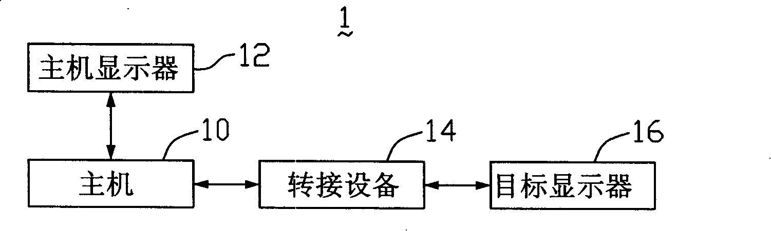
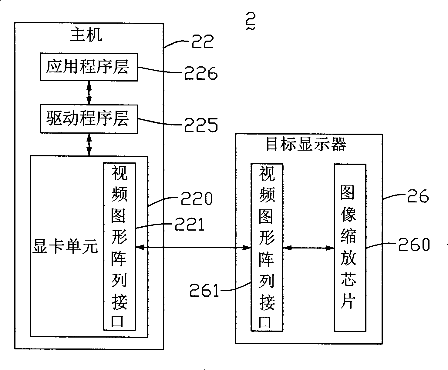
[0015] Please refer to figure 2 , which is a schematic structural diagram of a preferred embodiment of the display debugging system of the present invention. This display debugging system 2 comprises a main frame 22 and a target display 26, and this main frame 22 comprises a graphics card unit 220, a driver program layer 225 and an application program layer 226, and this graphics card unit 220 comprises a Video Graphics Array (Video GraphicsArray, VGA ) interface 221. The target display 26 is a liquid crystal display, which includes an image scaling chip 260 and a video graphics array interface 261 . The video graphics array interface 221 of the host 22 is connected to the video graphics array interface 261 of the target display 26 to realize the communication between the host 22 and the target display 26 . The application program layer 226 communicates with the driver program layer 225 through the I / O control channel, and the driver program layer 225 controls and drives th...


PUM


Abstract

The invention provides a display debug system and a debug method thereof. The display debug system of the invention comprises a host computer and a target display, wherein, the host computer comprises a graphics card unit, a driver layer and an application program layer; the graphic card unit comprises a video graphic array interface; the target display comprises an image zooming chip and a video graphic array interface; wherein, the application program layer comprises a plurality of chip type data and a graphic user interface; the host computer and the target display are connected and communicated with each other through the video graphic array interfaces of each other; the application program layer is communicated with the driver layer through an input and output control channel; the driver layer controls and drives the graphics card unit for reading and writing the image zooming chip; data of the image zooming chip is displayed on the target display through the graphic user interface; after modification and debugging, a debug result is directly displayed on the target display. The display debug system of the invention has the advantages of time saving and convenience of the display debug process and is universally used for a plurality of chips.

Description

technical field [0001] The invention relates to a display debugging system and a debugging method thereof, in particular to a liquid crystal display debugging system and a debugging method using the debugging system. Background technique [0002] Liquid crystal displays have been widely used in mobile phones, personal digital assistants, notebook computers, personal computers and televisions due to their low radiation, small size and low power consumption. Among them, in the process of firmware (Firmware) design of the liquid crystal display, debugging is one of the most important links. [0003] Please refer to figure 1 , which is a structural schematic diagram of a display debugging system in the prior art. The display debugging system 1 includes a host 10, a host display 12, an adapter device 14 and a target display 16, the target display 16 includes an image scaling chip (Scaling IC), and the host 10 is loaded with an image scaling chip. Corresponding test operating s...

Claims


Application Information

Patent Timeline
Patent Type & Authority Applications(China)
IPC IPC(8): G06F11/22G09G3/00G09G3/36G01R31/00G02F1/13
Inventor 黄光良代良燕曹统秀张晔王炜余言波
Owner INNOCOM TECH SHENZHEN
Why Eureka
Try Eureka