Drive device for image collecting system of interline transfer CCD sensor

A technology of an image acquisition system and a driving device, which is applied in the parts of TV systems, image communication, and color TV parts, etc., can solve the problems of difficult driver programming and circuit debugging, transmission distance and speed restrictions, and complex timing adjustment. And other issues

Inactive Publication Date: 2015-03-25
HARBIN ENG UNIV
View PDF6 Cites 11 Cited by
  • Summary
  • Abstract
  • Description
  • Claims
  • Application Information

AI Technical Summary

Problems solved by technology

However, in this method, the pulse timing cannot be directly generated by the main control chip like in the programmable logic device method. Due to the certain constraint relationship between the horizontal driving pulse, the vertical driving pulse and the analog-to-digital conversion sampling pulse, the timing adjustment is complicated, and the driving Program writing and circuit debugging are difficult
[0010] In the "Application No.: 201110100171.8" patent "Design of a CCD Spectral Model Universal Acquisition System Based on FPGA and USB2.0 Protocol Interface", the application of the traditional programmable logic device driving method is elaborated. This patent uses FPGA as the main control The device is also used as a CCD image sensor timing drive generator, using an independent AD conversion chip for analog-to-digital conversion, without making the timing generation circuit independent of the main control chip, only using hardware description language for all driver design and state machine for process control, Although it is convenient for driving timing control, it is too complicated for data reading, peripheral chip interface control and communication with the host computer, and the portability is poor. The output signal of the CCD image sensor is only processed by low-pass filtering, and the output of the image sensor is not fully considered. The characteristics of tiny signals; in this patent, the USB interface is used for data transmission, and its transmission distance and speed are limited to a certain extent

Method used


Image

  • Drive device for image collecting system of interline transfer CCD sensor
  • Drive device for image collecting system of interline transfer CCD sensor
  • Drive device for image collecting system of interline transfer CCD sensor

Examples


Embodiment Construction

[0030] The present invention will be described in further detail below in conjunction with the accompanying drawings.

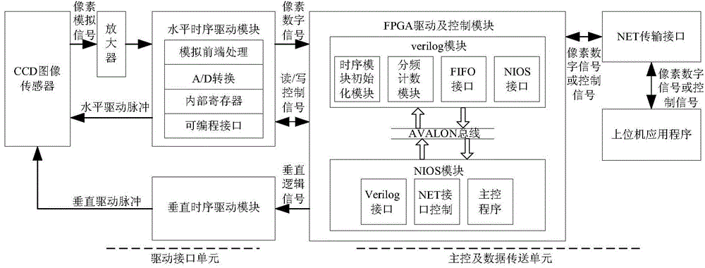
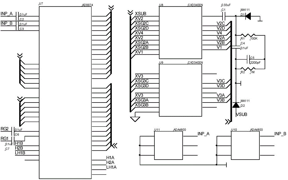
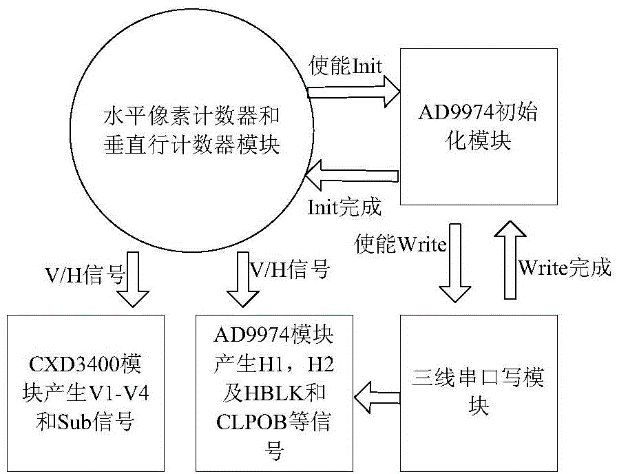
[0031] The design idea proposed by the invention can be applied to the driving design of inter-line transfer CCD image sensors that have different timing requirements. Such as figure 1As shown in the block diagram of the drive circuit, this design divides the circuit into two parts: the drive interface unit and the main control and data transmission unit. The drive interface unit outputs horizontal drive pulses and vertical drive pulses to the CCD image sensor. The pixel analog signal output by the CCD image sensor is amplified by the amplifier and then input to the horizontal timing drive module for analog front-end processing and analog-to-digital conversion. The converted pixel digital signal Send back to the FIFO interface sub-module inside the FPGA chip and wait for the host computer to accept the data. The FPGA chip of the main control and data transm...


PUM


Abstract

The invention discloses a drive device for an image collecting system of an interline transfer CCD sensor. The drive device comprises the CCD image sensor, a horizontal time sequence drive module, a vertical time sequence drive module, an FPGA drive and control module, an NET transmission interface and an upper computer. The FPGA drive and control module is connected with the horizontal time sequence drive module, the vertical time sequence drive module and the NET transmission interface. The NET transmission interface is connected with the upper computer for information exchange. The horizontal time sequence drive module generates horizontal drive pulses to the CCD image sensor. The vertical time sequence drive module generates vertical drive pulses to the CCD image sensor. The CCD image sensor outputs pixel simulation signals, and the pixel simulation signals are transmitted to the horizontal time sequence drive module through an amplifier. The horizontal time sequence drive module converts the pixel simulation signals to pixel digital signals and then transmits the pixel digital signals to the FPGA drive and control module. The drive device for the image collecting system of the interline transfer CCD sensor has the advantages of being high in flexibility and universality.

Description

technical field [0001] The invention belongs to a drive device for an image acquisition system, in particular to a CCD sensor, and is a drive device for an image acquisition system for an interline transfer CCD sensor. Background technique [0002] The image sensor is the most important part of the image acquisition system, and the success of its drive circuit design directly affects the performance of the entire image acquisition system. [0003] With the CCD image sensor as the core, the drive circuit scheme is selected first, and the drive circuit hardware design is carried out. Among the commonly used CCD image sensor drive schemes, the direct digital chip, EEPROM and single-chip microcomputer drive methods are suitable for CCD image sensors with low drive frequency and relatively simple timing. [0004] (1) Programmable logic device driving circuit [0005] Mainstream programmable logic devices include FPGA and CPLD, and FPGA is more suitable for sequential logic desi...

Claims


Application Information

Patent Timeline
Patent Type & Authority Applications(China)
IPC IPC(8): H04N5/372
Inventor 蔡成涛魏明岩吕晓龙夏桂华朱齐丹王立辉
Owner HARBIN ENG UNIV
Why Eureka
Try Eureka