Unlock instant, AI-driven research and patent intelligence for your innovation.

Inlaying inner connecting line structure and double inlaying process

A technology of dual damascene technology and damascene technology, which is applied in the field of dual damascene technology using metal mask layers and improved copper dual damascene technology, and can solve problems such as no way to solve residues

Active Publication Date: 2010-11-17
UNITED MICROELECTRONICS CORP
View PDF6 Cites 0 Cited by
  • Summary
  • Abstract
  • Description
  • Claims
  • Application Information

AI Technical Summary

Problems solved by technology

However, the above-mentioned patents still teach CH 2 f 2 or CHF 3 Plasma to remove, so there is no way to solve the problem of residue

Method used


Image

  • Inlaying inner connecting line structure and double inlaying process
  • Inlaying inner connecting line structure and double inlaying process
  • Inlaying inner connecting line structure and double inlaying process

Examples


Embodiment Construction

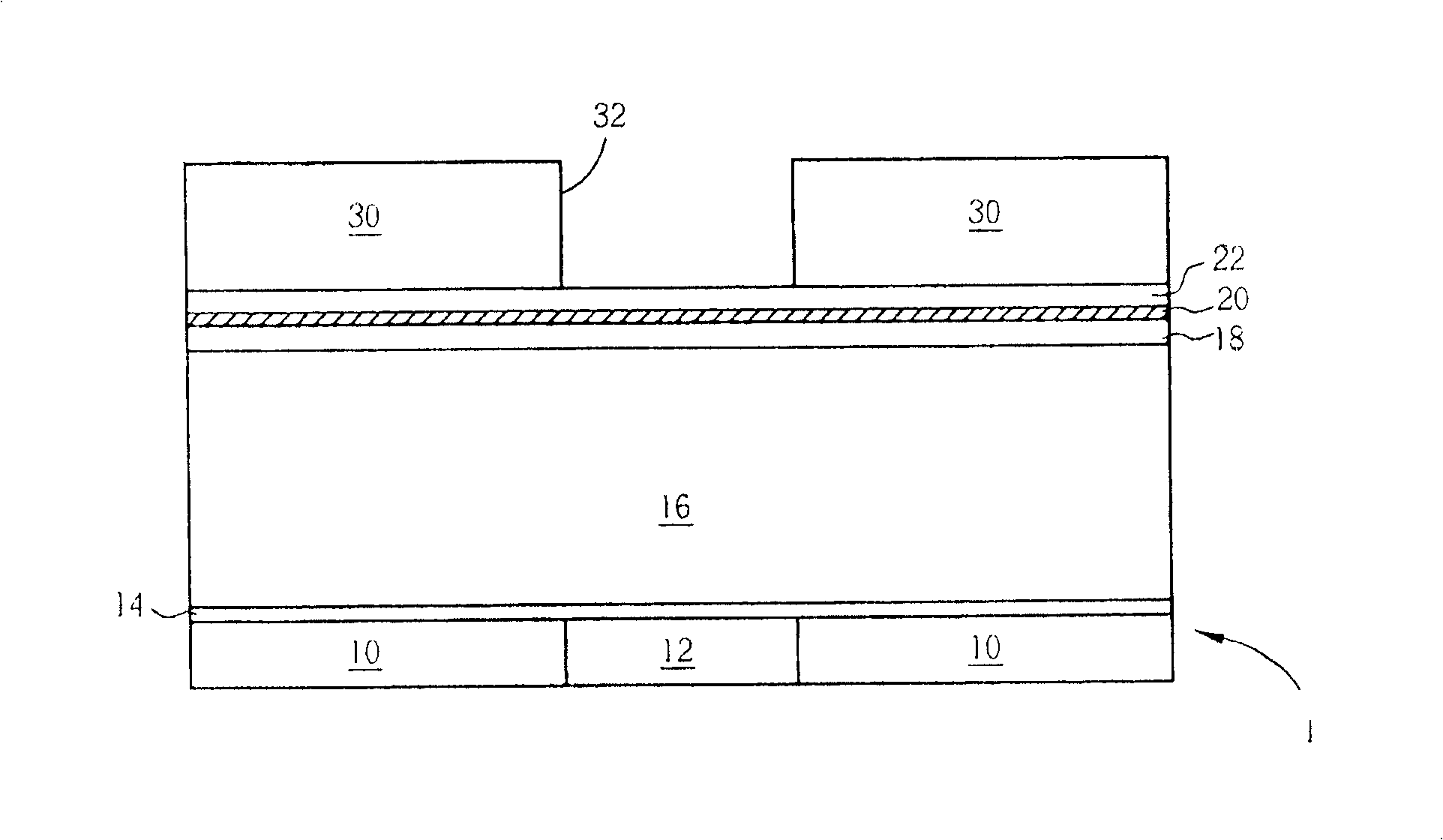
[0038] see Figure 9 to Figure 17 , which is a cross-sectional schematic diagram of a dual damascene process according to a preferred embodiment of the present invention, wherein the same symbols are still used to represent the same or similar components or regions. It should be emphasized that the present invention can be applied in trench-first, via-first, partial via-first and other damascene processes, and is not limited to those disclosed in the drawings .

[0039] Such as Figure 9 As shown, the substrate 1 is also provided with an underlying or low-k dielectric layer 10 . An underlying copper wire 12 is formed in the low-k dielectric layer 10 and covered with a capping layer 14 . According to a preferred embodiment of the present invention, the capping layer 14 is composed of silicon carbide (SiCN) doped with nitrogen, and has a thickness of about 300 to 800 angstrom, preferably about 500 angstrom. However, the capping layer 14 can also be made of other materials, s...


PUM

PropertyMeasurementUnit
thicknessaaaaaaaaaa
thicknessaaaaaaaaaa
thicknessaaaaaaaaaa

Abstract

The invention provides a dual damascene process. Firstly, a supporting base is provided and comprises a substrate dielectric layer, a conducting underlayer formed in the substrate dielectric layer and a covering layer covering the conducting underlayer and the substrate dielectric layer; subsequently, a dielectric layer is settled on the covering layer; a silica layer is settled on the dielectriclayer; a metallic hard mask is formed on the silica layer; then a trench is formed in the metallic hard mask; the silica layer and the dielectric layer are etched through the trench to form an access, thus exposing part of the covering layer. Finally, a liner is removed; the mixture plasma of hydrogenfree fluothane and a nitrogenous gas is used for selectively etching the covering layer exposed through the access, thus exposing part of the conducting underlayer.

Description

technical field [0001] The present invention relates to the field of copper interconnect semiconductor technology, in particular to an improved copper dual damascene (copper dual damascene) process, especially the use of metal hard mask (metal hard mask) dual damascene process, which can be used in the via When the misalignment with the underlying conductive lines occurs, it is avoided to simultaneously produce etching recess defects beside the underlying conductive lines due to the etching of the cap layer. Background technique [0002] As known to those skilled in the art, damascene interconnection technology is currently the mainstream technology used by the semiconductor industry to form copper wires in integrated circuits. In short, the manufacturing method of the inlaid interconnection structure is to etch the circuit pattern on the dielectric material film first, and then fill the copper metal into the pattern groove, and then etch the circuit pattern on the dielectri...

Claims


Application Information

Patent Timeline
Patent Type & Authority Patents(China)
IPC IPC(8): H01L21/768H01L21/311H01L23/522
Inventor 黄俊仁赖育聪姚志成廖俊雄
Owner UNITED MICROELECTRONICS CORP
Features
  • R&D
  • Intellectual Property
  • Life Sciences
  • Materials
  • Tech Scout
  • Unparalleled Data Quality
  • Higher Quality Content
  • 60% Fewer Hallucinations
Learn More