A package and manufacturing method for a microelectronic component

A technology of microelectronics and components, which is applied in the field of packaging of microelectronic components, and can solve the problems of easy damage of microelectronic devices and contamination of bonding pads, etc.

A technology of microelectronics and components, which is applied in the field of packaging of microelectronic components, and can solve the problems of easy damage of microelectronic devices and contamination of bonding pads, etc.

CN101233619BActive Publication Date: 2012-02-15NXP BV

Image

  • A package and manufacturing method for a microelectronic component
  • A package and manufacturing method for a microelectronic component
  • A package and manufacturing method for a microelectronic component

Examples


Embodiment Construction

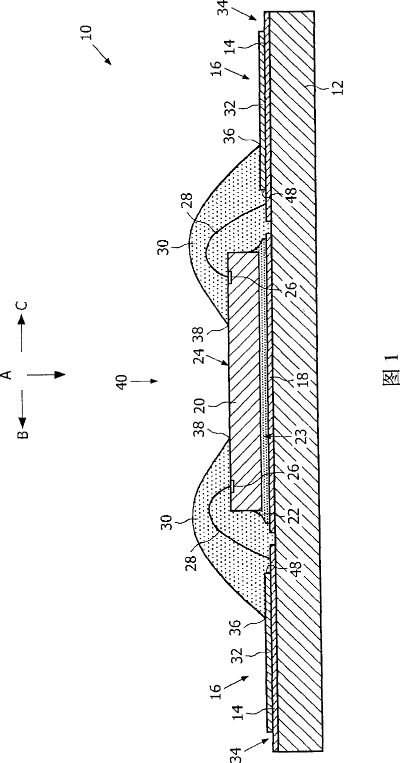
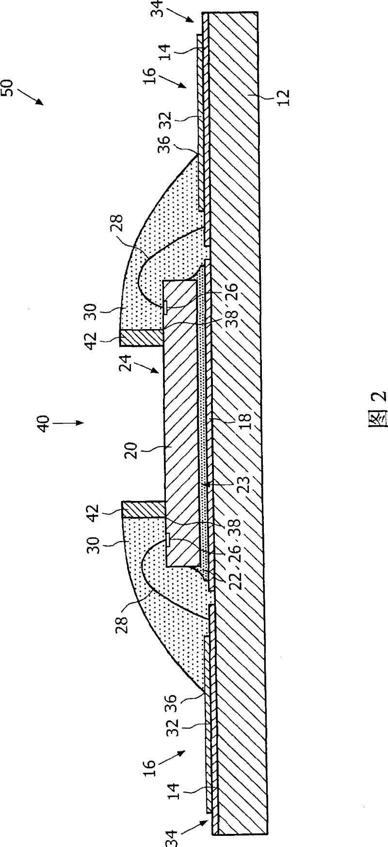
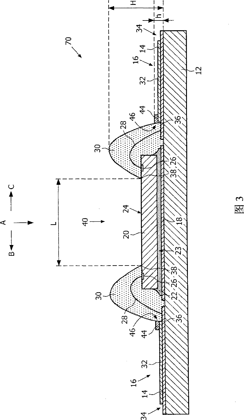
[0033] exist image 3 , a cross-sectional view of package 70 is shown along the Figure 4b Intercepted at line 3-3. The package 70 includes a dam 44 provided on the outer layer 32 on the first side. The dam includes a stepped surface transition 46 between the outer layer 32 and the conductor 14 or layer 49 below the outer layer (see Figure 4a with Figure 4b )between. During the curing of the glob material 30 , the dam affects the shape of the glob material 30 to expand the width L of the central region 40 and thus the surface area of ​​the central region. Process each inner edge 48 of the outer layer 32 (see figure 1 ), facing the sealing material in place and applying an additional layer on top of the layer 32 parallel to said edge of the layer 32, thereby forming a dam 44, as image 3 shown. Another solution is to arrange the edge 48 of the outer layer 32 closer to the outside of the carrier element 12, and an additional layer is applied on top of the conductive tra...


PUM


Abstract

The present invention relates to A package (50,70) for a microelectronic component, comprising: a carrier element (12) having a first side (16) that comprises conductor lines (14); -a microelectronic component (20) having a first surface (24) and a second surface (23) facing away from the first surface; the microelectronic component with said second surface mounted on said first side and connected to the conductor lines via bonding wires (28); a polymeric encapsulation material (30) encapsulating the bonding wires and exposing a central zone (40) of said first surface (24), the encapsulation material comprising an outer edge (36) at said first side and an inner edge (38) at said first surface; a dam (42,44) abutting to the encapsulation material; wherein the dam (44) comprises a step-shaped surface transition (46) at said first side (16), the surface transition abutting on said outer edge (36). The dam (44) influences the forming of the outer (36) and the inner edge (38) during manufacturing the encapsulation material (30) and enlarges the area of the central zone (40). The present invention also relates to a method of manufacturing such a package for a microelectronic component.

Description

technical field [0001] The invention relates to a package of microelectronic components, comprising: a carrier element with leads; a microelectronic component mounted on the carrier element and connected to the leads via bonding wires; and an encapsulation material for The bonding wires are sealed and the central region of the upper surface of the microelectronic component is exposed. Background technique [0002] Such packaging of microelectronic components is well known. Two common designs of such packages known in the art are described below to give an introduction to the present invention. exist figure 1 with 2 These designs are shown in , where the same reference numbers indicate the same or similar parts. figure 1 A schematic cross-sectional view of a package showing a microelectronic component. Package 10 includes a carrier element 12 having a first side 16 including leads 14 . Microelectronic component 20 is mounted on die pad 18 of the substrate by adhesive 22...

Claims


Application Information

Patent Timeline
15 Feb 2012
Publication
CN101233619B
IPC
H01L31/0203; H01L21/56; H01L23/31; H01L33/00; H01L27/146; B81B7/00; B81C5/00; H05K3/00; H05K3/28; G06K9/00; B81C99/00; H01L33/52; H01L33/54
CPC
H01L31/0203; G01N27/128; H01L2924/1815; H01L2224/73265; H01L2224/45144; H01L2224/32225; G01P1/023; B81C1/00333
Inventors
丹迪·N·扎杜卡纳; 乔纳森·S·卡塔拉