
Serrated Fourier filters and inspection systems

一种滤波器、傅立叶的技术,应用在仪器、科学仪器、测量装置等方向,能够解决不能提供性能等问题

Inactive Publication Date: 2008-08-06
KLA TENCOR TECH CORP
View PDF0 Cites 2 Cited by
  • Summary
  • Abstract
  • Description
  • Claims
  • Application Information

AI Technical Summary

Problems solved by technology

Fourier filters made in this way are relatively cheap, but do not provide the desired performance

Method used


Image

  • Serrated Fourier filters and inspection systems
  • Serrated Fourier filters and inspection systems
  • Serrated Fourier filters and inspection systems

Examples


Embodiment Construction

[0036] DETAILED DESCRIPTION OF THE PREFERRED EMBODIMENT

[0037] As used herein, the term "wafer" generally refers to a substrate formed of semiconductor or non-semiconductor material. Examples of such semiconducting or non-semiconducting materials may include, but are not limited to, monocrystalline silicon, gallium arsenide, and indium phosphide. Such substrates are commonly found and / or processed in semiconductor fabrication facilities. A wafer may include one or more layers formed on a substrate. For example, these layers may include, but are not limited to: resists, dielectric materials, and conductive materials. Many different types of such layers are known in the art, and the term wafer as used herein is intended to include all types of such layers.

[0038] One or more layers formed on the wafer may or may not be patterned. For example, a wafer may include multiple die, each die having repeatable patterned features. Formation and processing of such material layers...


PUM


Abstract

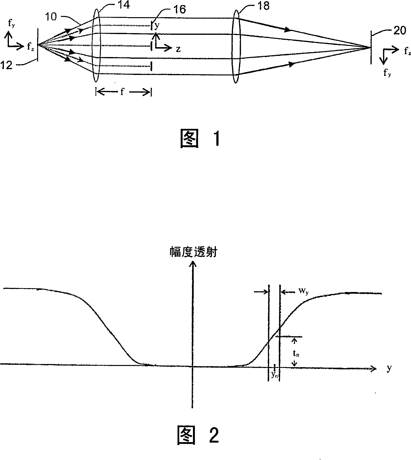
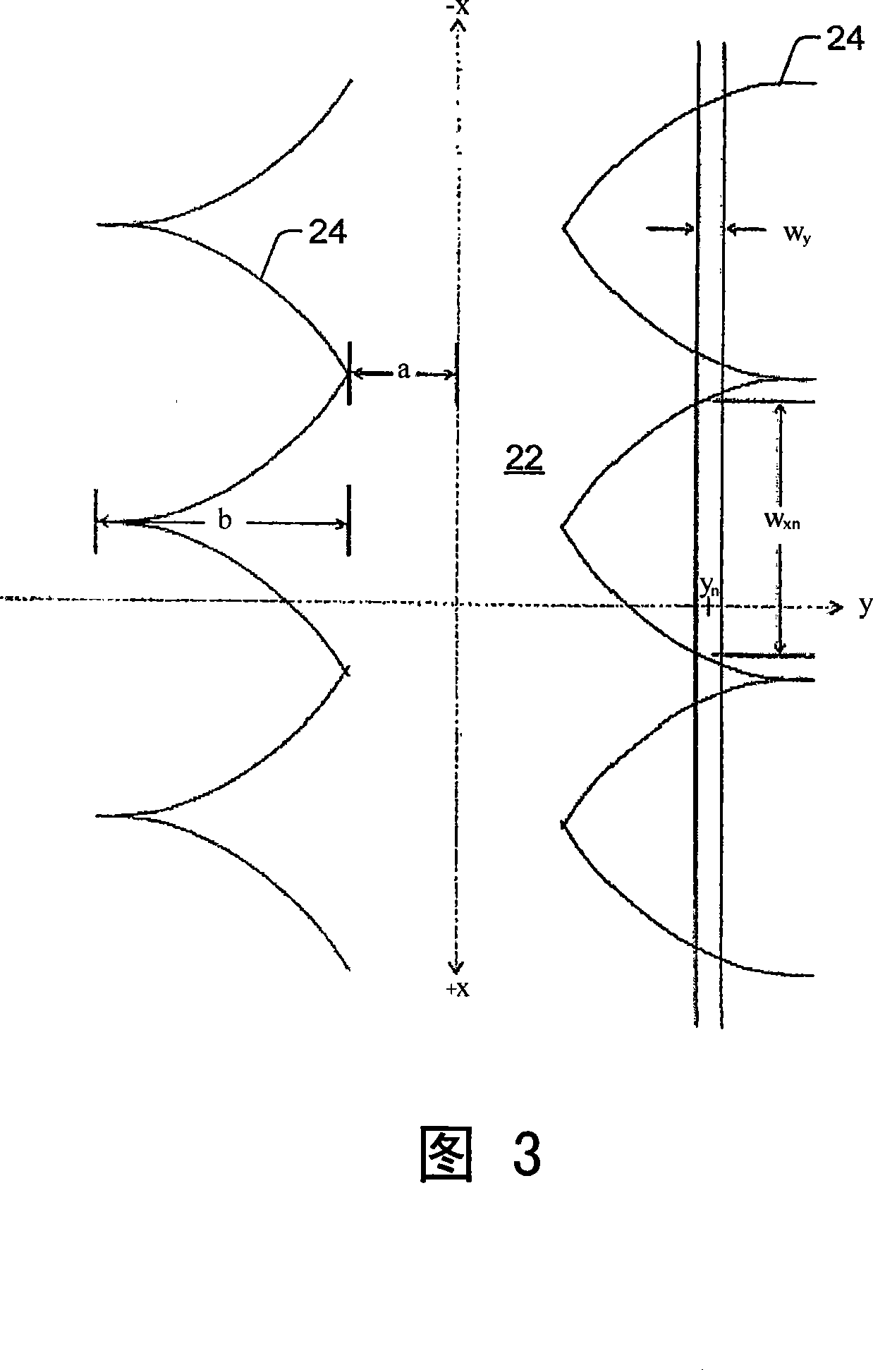
A sawtooth Fourier filter and inspection system is provided. A Fourier filter includes one or more blocking elements configured to block a portion of light from a wafer. The Fourier filter further includes periodic sawtooth formed on edges of the one or more blocking units. The periodic serrations define a transition section of the one or more barrier elements. The periodic sawtooth is configured to vary the transmission across the transition section such that the variation of the transmission across the transition section is substantially smooth. An inspection system includes a Fourier filter configured as described above and a detector configured to inspect light transmitted by the Fourier filter. The signal generated by the detector may be used to detect the defect on the wafer.

Description

Background of the invention [0001] 1. Field of invention [0002] The present invention relates generally to serrated Fourier filters and inspection systems. Some embodiments relate to a Fourier filter comprising periodic sawtooth formed at the edge of one or more blocking elements and configured to increase across one or more blocking elements. The smoothness of the transmission change of the transition region of the barrier unit. [0003] 2. Description of prior art [0004] The following description and examples are not admitted to be prior art by inclusion in this section. [0005] Fabrication of semiconductor devices, such as logic and memory devices, typically involves processing a substrate, such as a semiconductor wafer, using a number of semiconductor fabrication processes to form various features and layers of the semiconductor device. For example, photolithography is a semiconductor fabrication process that typically involves transferring a pattern from a mas...

Claims


Application Information

Patent Timeline
Patent Type & Authority Applications(China)
IPC IPC(8): G01N21/00
CPCG01N21/95623
Inventor H·J·郑A·V·希尔M·S·王
Owner KLA TENCOR TECH CORP
Features
  • Generate Ideas
  • Intellectual Property
  • Life Sciences
  • Materials
  • Tech Scout
  • Unparalleled Data Quality
  • Higher Quality Content
  • 60% Fewer Hallucinations
Learn More