Device and method for integrating basic electric property and system function detection

A technology of electrical testing and testing equipment, which is applied in the direction of measuring equipment, electronic circuit testing, and electrical measurement, and can solve problems such as increased testing costs, reduced production capacity, and extended batch operation time

Inactive Publication Date: 2008-09-24
KING YUAN ELECTRONICS
View PDF0 Cites 4 Cited by
  • Summary
  • Abstract
  • Description
  • Claims
  • Application Information

AI Technical Summary

Problems solved by technology

Since the basic electrical test does not require many tedious testing processes like the functional test, only a simple electrical test is required to prevent the test machine from being damaged during the test. Obviously, the basic electrical test takes a long time. The time required for the functional test is less than that of the functional test, so the semiconductor testing device is only equipped with a mechanical arm to handle the basic electrical test of the DUT and the transfer operation of the functional test, and the mechanical arm is required to continuously move the DUT for a long distance between the two. Prolonging the operation time of the batch reduces the throughput, and as the number of times the DUT is transferred increases, the number of times the DUT contacts the socket also increases, so that the damage rate of the DUT also increases , and lead to an increase in test cost

Method used


Image

  • Device and method for integrating basic electric property and system function detection
  • Device and method for integrating basic electric property and system function detection
  • Device and method for integrating basic electric property and system function detection

Examples


Embodiment Construction

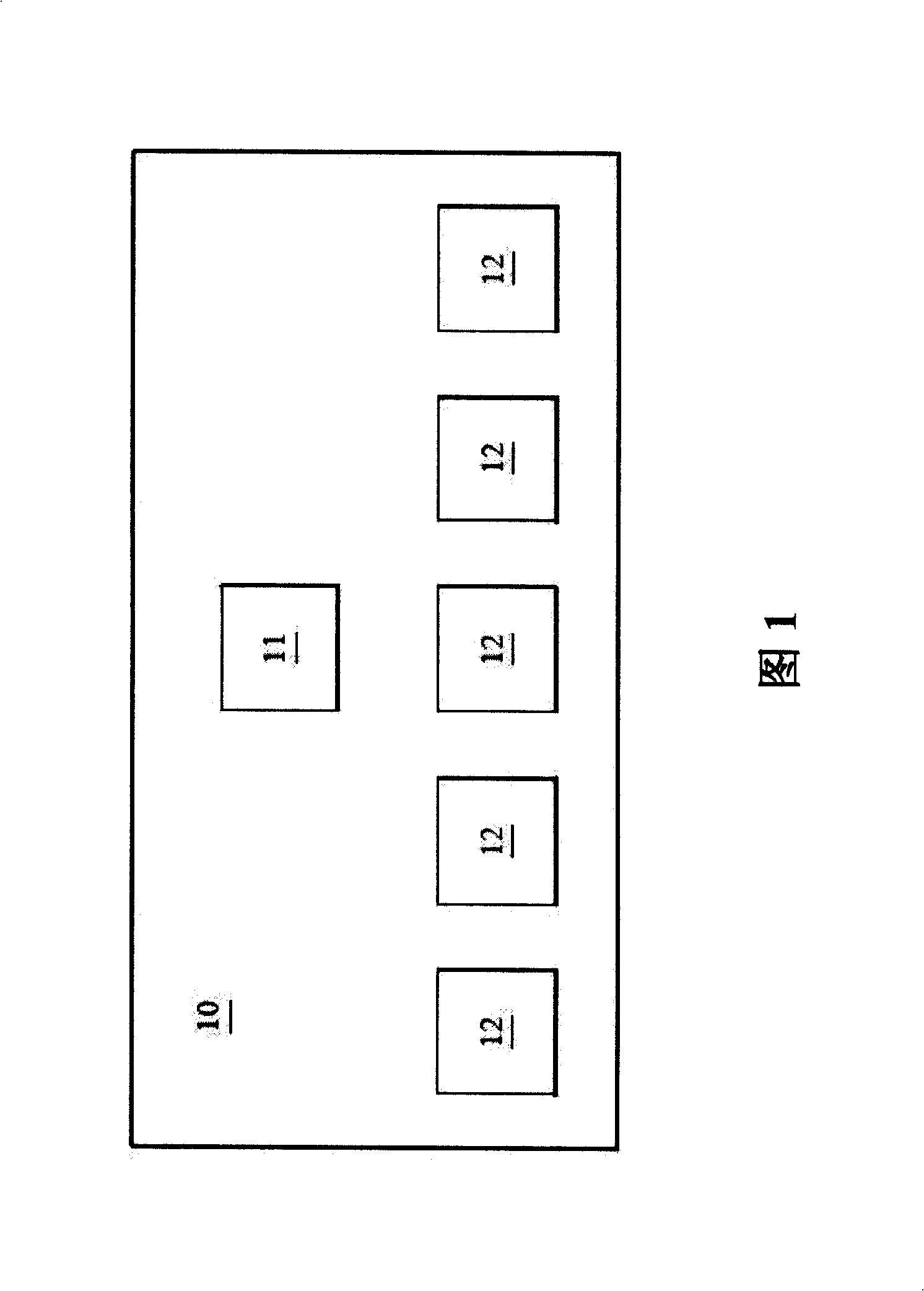
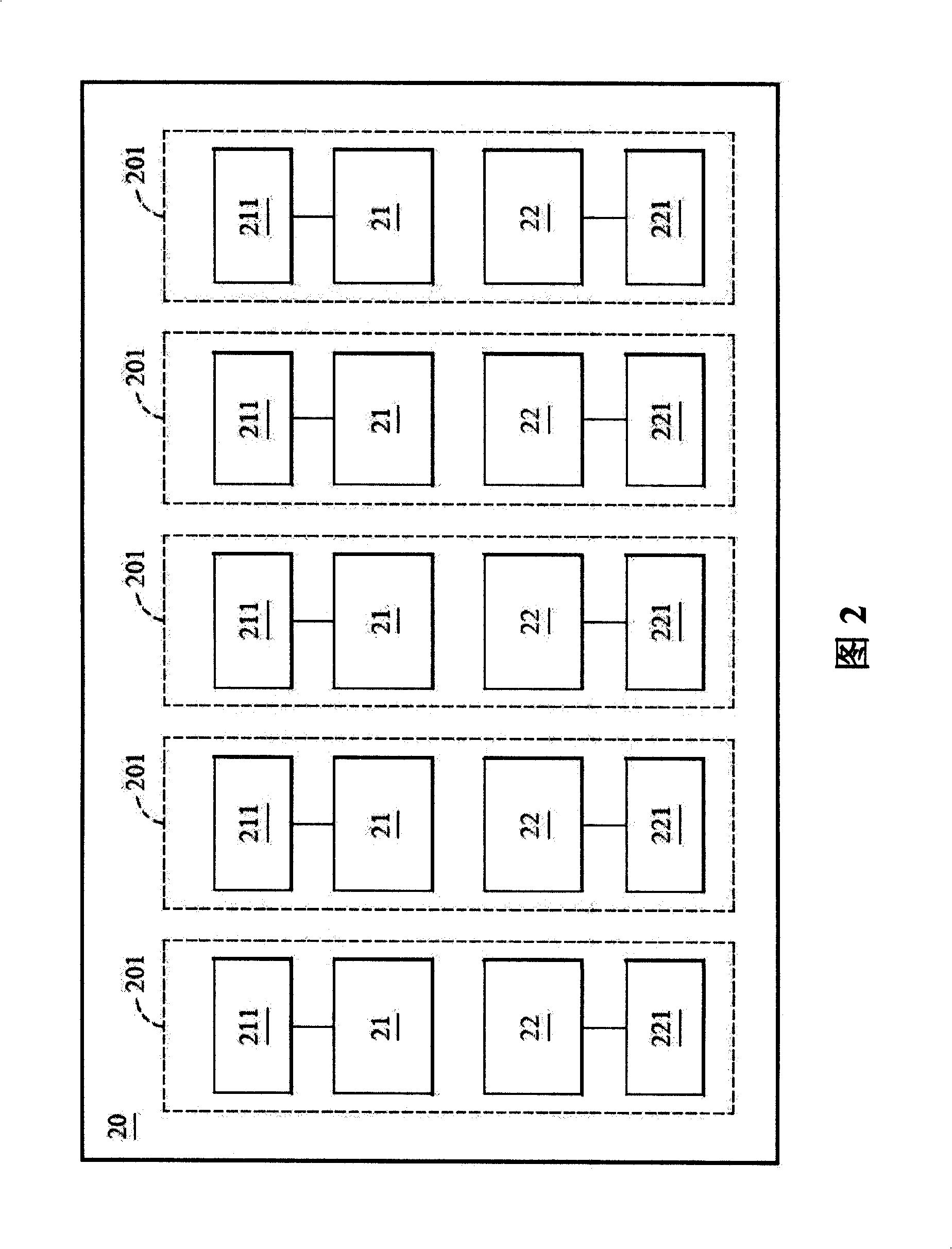
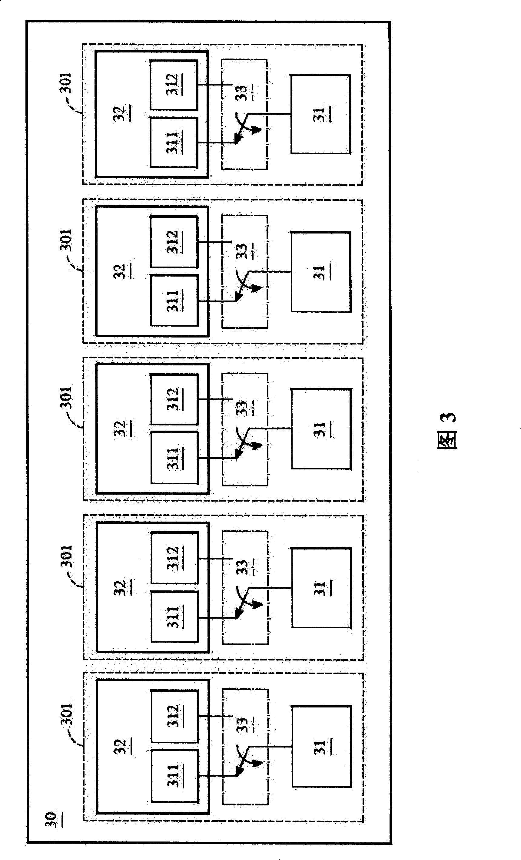
[0026] The direction discussed in the present invention is the setting of a test area integrating basic electrical and functional testing in a semiconductor testing device. In order to thoroughly understand the present invention, detailed steps and composition methods will be proposed in the following description. Obviously, the implementation of the present invention is not limited to the specific details familiar to the technicians of the basic electrical and system function testing test device. On the other hand, the settings or test procedures of the well-known semiconductor testing device are not described in details to avoid unnecessary limitations of the present invention. The preferred embodiments of the present invention will be described in detail as follows. However, in addition to these detailed descriptions, the present invention can also be widely implemented in other embodiments, and the scope of the present invention is not limited, and the claims shall prevail.

...


PUM


Abstract

The invention provides a testing device which integrates basic electrical property and system function detection, and a testing method. By integrating a basic electrical property testing circuit and a system function circuit on the same circuit substrate and by the effect of element shifting, the element to be tested which passes the test of basic electrical property test can directly carry out the test of system function on the same slot, thus effectively saving the working time for testing, and reducing the damage rate of the element to be tested.

Description

Technical field [0001] The present invention relates to a setting of a semiconductor test device and a test method thereof, in particular to a setting and a test method of integrating basic electrical test and function test on the same circuit substrate. Background technique [0002] The semiconductor test manufacturing process is to perform electrical functional tests on ICs (also called components under test) to ensure the integrity of IC functions and to perform IC classification according to test results. However, in order to ensure that the test circuit will not be damaged due to the poor state of the component under test, it is necessary to perform basic electrical tests, such as open / short circuit test, and determine the component under test. After the basic electrical properties are normal, with the assistance of the robotic arm of the sorter, the component to be tested is transported to the functional test area for testing or system function testing. [0003] Please refe...

Claims


Application Information

Patent Timeline
IPC IPC(8): H01L21/66G01R31/00G01R31/26G01R31/28
Inventor 林源记谢志宏林世芳潘浩欣
Owner KING YUAN ELECTRONICS
Why Eureka
Try Eureka