Wafer structure of projection definization

A bump and chip technology, applied in the field of semiconductor wafer structure, can solve the problems of general products without suitable structure, inconvenience, weakening of bump bonding strength, etc.

Active Publication Date: 2008-09-24
ULTRA CHIP INC
View PDF0 Cites 4 Cited by
  • Summary
  • Abstract
  • Description
  • Claims
  • Application Information

AI Technical Summary

Problems solved by technology

When the number of the bumps 120 is required to increase, the size of the bumps 120 is reduced synchronously, resulting in weakening of the bonding strength of the bumps.
[0009] It can be seen that the above-mentioned existing bumped wafer structure obviously still has inconvenience and defects in structure and use, and needs to be further improved urgently.
In order to solve the above-mentioned problems, the relevant manufacturers have tried their best to find a solution, but for a long time no suitable design has been developed, and the general products do not have a suitable structure to solve the above-mentioned problems. Urgent problem

Method used


Image

  • Wafer structure of projection definization
  • Wafer structure of projection definization
  • Wafer structure of projection definization

Examples


Embodiment Construction

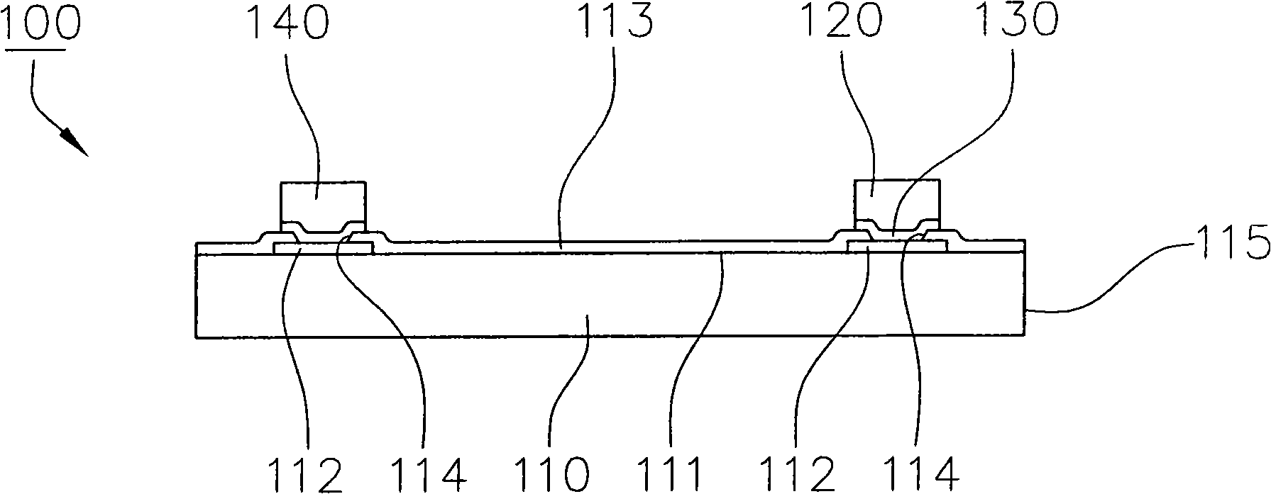
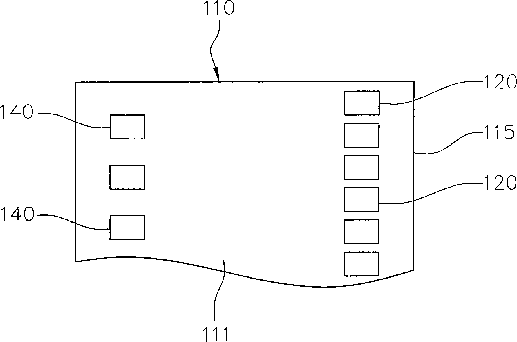
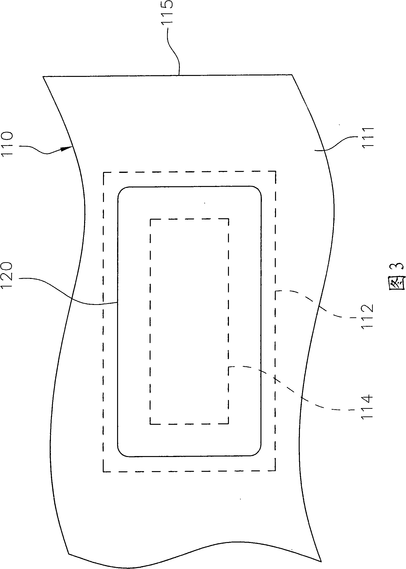
[0045] In order to further explain the technical means and effects that the present invention adopts to achieve the intended purpose of the invention, below in conjunction with the accompanying drawings and preferred embodiments, the specific implementation, structure, and characteristics of the chip structure of bump fingering proposed according to the present invention will be described below. And its effect, detailed description is as follows.

[0046] see Figure 4 and Figure 5 as shown, Figure 4 It is a schematic cross-sectional view of a bump-fingered wafer structure according to a specific embodiment of the present invention; Figure 5 is a partial schematic diagram of the top surface of the bump fingered wafer structure. According to a specific embodiment of the present invention, a wafer structure with bump fingering is disclosed. The bump-fingered chip structure 200 mainly includes a chip body 210 and a plurality of finger-shaped bumps 220 and / or bumps 240 .

...


PUM


Abstract

The invention relates to a wafer structure of bump fingerization, which mainly comprises a wafer body and a plurality of fingery bumps. The wafer body is provided with a plurality of connecting pads. The fingery bumps are arranged on the wafer body with bump shapes, each fingery bump is provided with a bump block and an extension part, the bottom covering area of the bump blocks is arranged in the connecting pads, and the bottom covering area of the extension parts is beyond the connecting pads. Therefore, under the condition of not increasing the size of the wafer, more fingery bumps can be collocated in micro-interval, and bonding strength of the bumps can not be influenced.

Description

technical field [0001] The invention relates to a semiconductor wafer structure, in particular to a bump that can be configured with more finger-shaped bumps without increasing the size of the wafer, without affecting the bonding strength of the bumps, and can meet the requirements for high-density arrangement of bumps Refers to the crystallized wafer structure. Background technique [0002] Metal bumps, such as gold bumps, are made on the pads of integrated circuit chips to facilitate external electrical connection, and to facilitate subsequent application in chip-on-glass (COG, Chip On Glass) and chip-on-thin film packaging (COF, Chip On Film) and other semiconductor products. The electronic signal is transmitted to the matching device through the bumps and substrate leads located on both sides of the integrated circuit chip, such as a liquid crystal display. With the high image quality and high resolution required by the display, the number of bumps required by the chip ...

Claims


Application Information

Patent Timeline
IPC IPC(8): H01L23/485H01L23/50
CPCH01L24/14H01L2224/14051H01L2224/14H01L2924/14H01L2924/00H01L2924/00012
Inventor 施合成王俊元郑怡芳王琼琳锺孙雯
Owner ULTRA CHIP INC
Why Eureka
Try Eureka