Wafer structure possessing finger-like projection connected with multi-window

A bump and wafer technology, applied in the field of bumped semiconductor wafer structures, can solve the problems of reduced top surface bonding area, weakened bump bonding strength, general products without suitable structures, etc.

Inactive Publication Date: 2008-11-26
ULTRA CHIP INC
View PDF0 Cites 1 Cited by
  • Summary
  • Abstract
  • Description
  • Claims
  • Application Information

AI Technical Summary

Problems solved by technology

When the number of the bumps 120 is required to increase, the bonding area of ​​the top surfaces of the bumps 120 is also reduced synchronously, resulting in weakening of the bonding strength of the bumps.
[0006] It can be seen that the above-mentioned existing bumped wafer structure obviously still has inconvenience and defects in structure and use, and n

Method used


Image

  • Wafer structure possessing finger-like projection connected with multi-window
  • Wafer structure possessing finger-like projection connected with multi-window
  • Wafer structure possessing finger-like projection connected with multi-window

Examples


no. 1 Embodiment

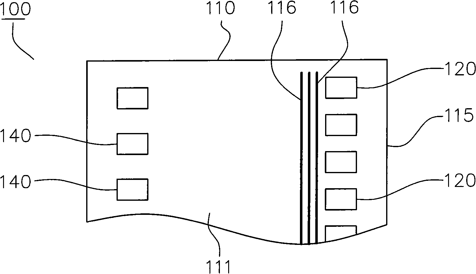
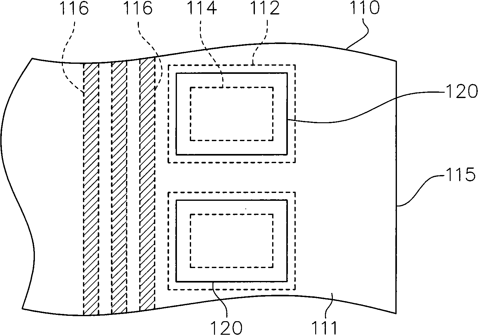
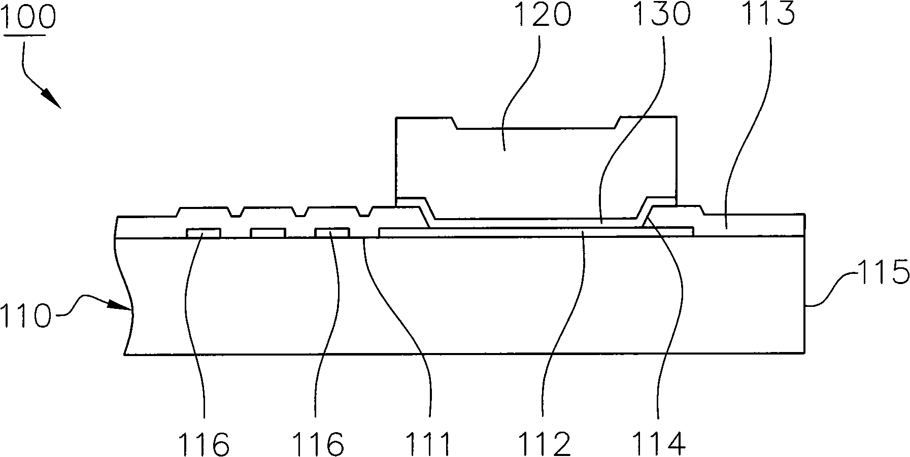
[0109] According to a first embodiment of the present invention, a wafer structure having fingered bumps bonded to multiple openings is disclosed. Fig. 4 is a partial schematic diagram of the top surface of the wafer structure, Fig. 5 is an enlarged schematic diagram showing the top surface of the finger-shaped bump of the wafer structure, Fig. 6 is a schematic cross-sectional diagram of the finger-shaped bump of the wafer structure, and Fig. 7 is a diagram illustrating A partial cross-sectional enlarged schematic view of the wafer structure bonded to a substrate at the finger-shaped bumps.

[0110] Referring to FIGS. 4 to 6 , a chip structure 400 with fingered bumps bonded to multi-opening windows according to the first embodiment of the present invention mainly includes a chip body 410 and a plurality of fingered bumps 420 .

[0111] The chip body 410 mentioned above, as shown in FIG. 6 , has an active surface 411 and a plurality of pads 412 disposed on the active surface 4...


PUM

PropertyMeasurementUnit
Thicknessaaaaaaaaaa
Heightaaaaaaaaaa
Lengthaaaaaaaaaa

Abstract

The invention relates to a chip structure having fingerlike bumps bonded on multi-windows. The fingerlike bumps are arranged on a chip body having a plurality of pads and a surface protective layer, the surface protective layer is provided with a plurality of openings locally exposing each pad, and the openings can be in linear arrangement, parallel arrangement or rectangular arrangement. The fingerlike bumps in the shape of a projection are arranged on the chip body, each fingerlike bump is provided with a bump body and an extension portion, a covering area of the bottom of the bump body is located in the corresponding pad for covering the corresponding group of openings, and the covering area of the bottom of the extension portion is arranged over the pads for maintaining joint strength of the bumps with fine pitches. In an embodiment, the covering areas of the bottom of the extension portions cross at least one tracing line. The chip structure meets the requirements on the fin pitches of the bumps or/and high-density arrangement without affecting the joint strength of the bumps. The chip structure can increase the amount of joints of the pads of the chip, increases the crack resistant property of the bottom of the bumps, disperses skin areas on the top of the bumps, and can increase the joint strength of the bumps.

Description

technical field [0001] The present invention relates to a bumped semiconductor wafer structure, in particular to a structure that can meet the requirements of fine-pitch or / and high-density arrangement of bumps, and can also improve the joint strength of bumps and has a finger jointed on multiple windows. IC CHIP HAVING FINGER-LIKE BUMPSBONDED ON MULTI-WINDOWS. Background technique [0002] Metal bumps, such as gold bumps, are made on the pads of integrated circuit chips to facilitate external electrical connection, and to facilitate subsequent application in chip-on-glass (COG, Chip On Glass) and chip-on-thin film packaging (COF, Chip On Film) and other semiconductor products. The electronic signal is transmitted to the matching device through the bumps and substrate leads located on both sides of the integrated circuit chip, such as a liquid crystal display. With the high image quality and high resolution required by the display, the number of bumps required by the chip ...

Claims


Application Information

Patent Timeline
IPC IPC(8): H01L23/485
CPCH01L2924/0002H01L2224/13
Inventor 施合成王俊元郑怡芳王琼琳锺孙雯
Owner ULTRA CHIP INC
Why Eureka
Try Eureka