Integrated circuit package body and manufacturing method thereof

A technology of an integrated circuit and a manufacturing method, which is applied to an integrated circuit package body with a high pass rate and its manufacturing field, can solve the problems of reducing the pass rate of the integrated circuit package body and the like.

Inactive Publication Date: 2008-10-01
XINTEC INC
View PDF0 Cites 19 Cited by
  • Summary
  • Abstract
  • Description
  • Claims
  • Application Information

AI Technical Summary

Problems solved by technology

like Figure 1D As shown, the adhesive 10 will overflow to the area of ​​the photosensitive element 12, and cover part of the photosensitive element 12, thus resulting

Method used


Image

  • Integrated circuit package body and manufacturing method thereof
  • Integrated circuit package body and manufacturing method thereof
  • Integrated circuit package body and manufacturing method thereof

Examples


Embodiment Construction

[0066] Next, the present invention will be described in detail with embodiments and accompanying drawings. In the drawings or descriptions, similar or identical parts use the same symbols. In the drawings, the shape or thickness of the embodiments may be exaggerated to simplify or facilitate labeling. Parts of the elements in the drawings will be explained in the description. It is to be understood that elements not shown or described may have various forms well known to those skilled in the art. In addition, when it is described that a layer is on a substrate or another layer, the layer may be directly on the substrate or another layer, or there may be an intervening layer therebetween.

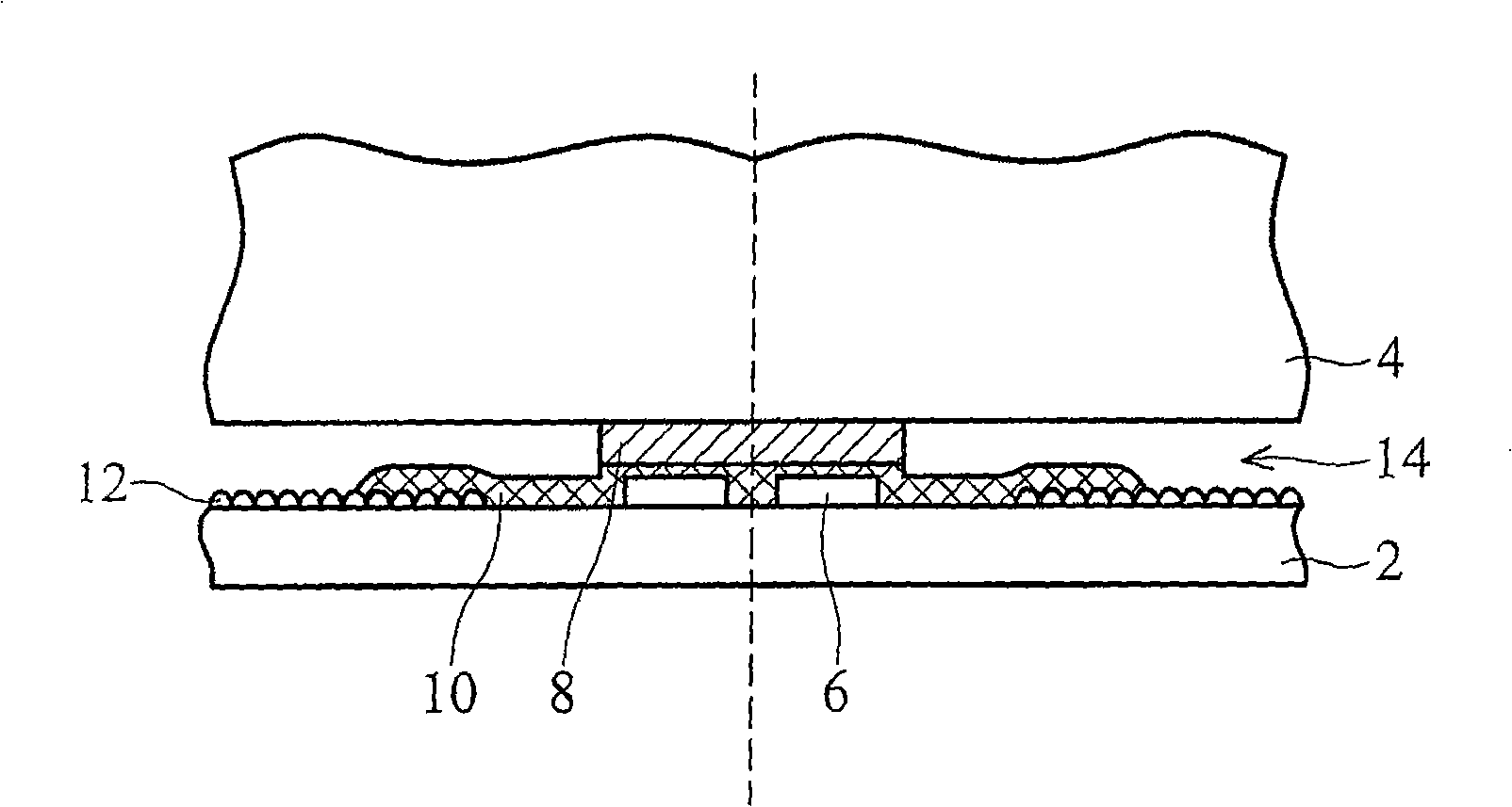
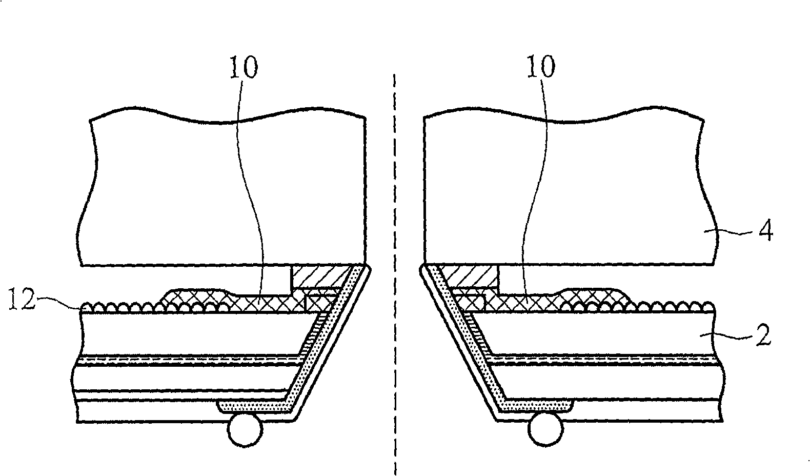
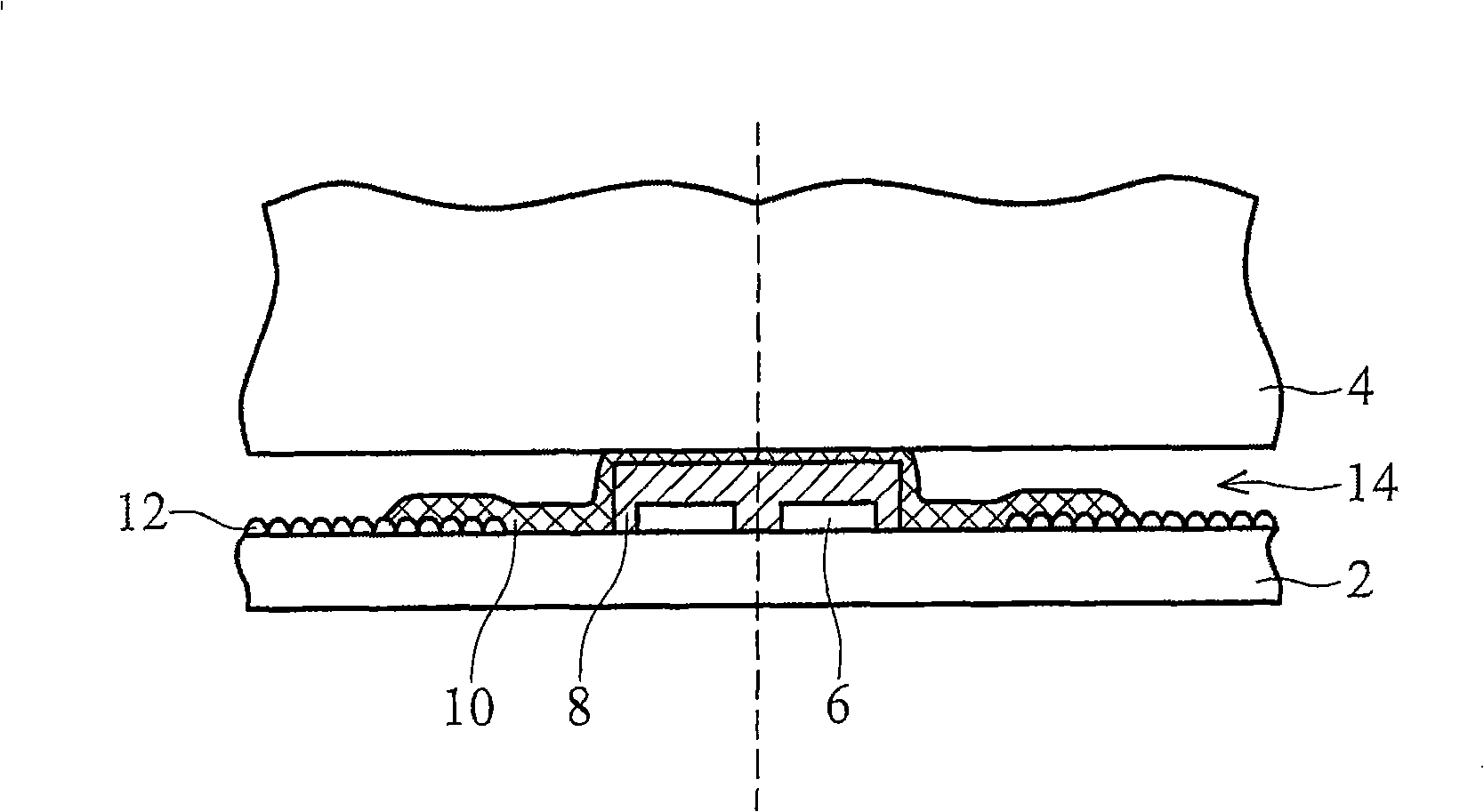
[0067] exist Figure 2A-Figure 2H A cross-sectional view of an integrated circuit package fabricated according to the first embodiment of the present invention is shown in . exist Figure 2A In the present invention, an integrated circuit chip 102 having an upper surface 103 and a lower ...


PUM


Abstract

The invention provides an integrated circuit package body and a manufacturing method thereof. The integrated circuit package body comprises an integrated circuit chip whose upper surface is formed with a sensitive element; a joint bonding pad formed on the upper surface of the integrated circuit chip and connected with the sensitive element electrically; a first blocking wall formed between the sensitive element and the joint bonding pad; and a conductive layer formed on the sidewall of the integrated circuit chip and connected with the joint bonding pad electrically. The first blocking wall of the invention can block the bonding agent to overflow to the area of the sensitive element, improving the qualified rate of manufacturing process of the integrated circuit package body.

Description

technical field [0001] The invention relates to an integrated circuit packaging body and a manufacturing method thereof, in particular to an integrated circuit packaging body with a high pass rate and a manufacturing method thereof. Background technique [0002] In the manufacturing process of integrated circuit devices, the integrated circuits must be packaged and used in various application fields, such as computers, mobile phones or digital cameras. Therefore, the yield of integrated circuit packaging also directly affects the yield of final integrated circuit devices. [0003] Figure 1A-Figure 1D A cross-sectional view showing an existing integrated circuit package. like Figure 1A and Figure 1B The form in which the protective layer 8 is formed on the cover plate 4 before the bonding step is shown. and Figure 1C and Figure 1D The form in which the protective layer 8 is formed on the integrated circuit chip 2 before the bonding step is shown. exist Figure 1A...

Claims


Application Information

Patent Timeline
IPC IPC(8): H01L27/14H01L23/485H01L21/60
CPCH01L2224/10
Inventor 颜裕林范振梅
Owner XINTEC INC
Why Eureka
Try Eureka