

Method for forming threading hole on substrate
A technology of through holes and silicon substrates, which is applied in semiconductor/solid-state device manufacturing, electrical components, circuits, etc., and can solve problems such as uneven thickness and inconsistent capacitance
- Summary
- Abstract
- Description
- Claims
- Application Information
AI Technical Summary
Problems solved by technology
Method used
Image

Examples
Embodiment Construction
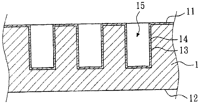
[0011] refer to Figure 4 to Figure 19 , is a schematic diagram showing a first embodiment of the method for forming a through hole on a substrate according to the present invention. refer to Figure 4 and Figure 5 ,in Figure 4 is the top view of the substrate, Figure 5 for Figure 4 A cross-sectional view along line 5-5. Firstly, a substrate 2 is provided, and the substrate 2 has a first surface 21 and a second surface 22 . The substrate 2 is, for example, a silicon substrate or a wafer. Next, a first photoresist layer 23 is formed on the first surface 21 of the substrate 2 , and a first opening 231 is formed on the photoresist layer 23 . In this embodiment, the first opening 231 is circular in plan view. It can be understood that the first opening 231 may also be square in plan view.
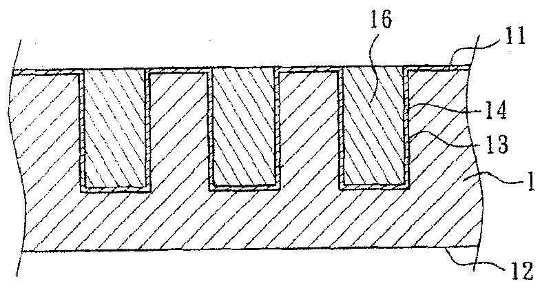
[0012] Next, refer to Image 6 A groove 24 is formed on the substrate 2 according to the first opening 231 by etching or other methods, and the groove 24 does not penetrate the sub...
PUM
 Abstract
Description
Claims
Application Information