Wafer level semiconductor package with dual side build-up layers and method thereof
A semiconductor, wafer-level technology, applied in the field of wafer-level packaging structure, can solve problems such as cost increase
- Summary
- Abstract
- Description
- Claims
- Application Information
AI Technical Summary
Problems solved by technology
Method used
Image

Examples
Embodiment Construction
[0046] The present invention will be described in detail below with its preferred embodiments and accompanying drawings. It should be understood that all the preferred embodiments in the present invention are for illustration only, not for limitation. Therefore, except for the preferred embodiment herein, the present invention can also be widely applied in other embodiments. And the present invention is not limited to any embodiment, and should be determined by the scope of the attached patent application and its equivalent fields.
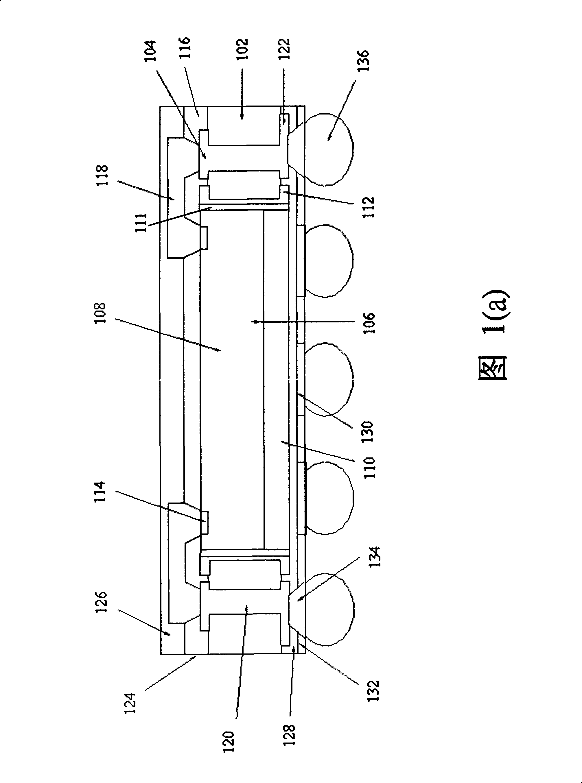
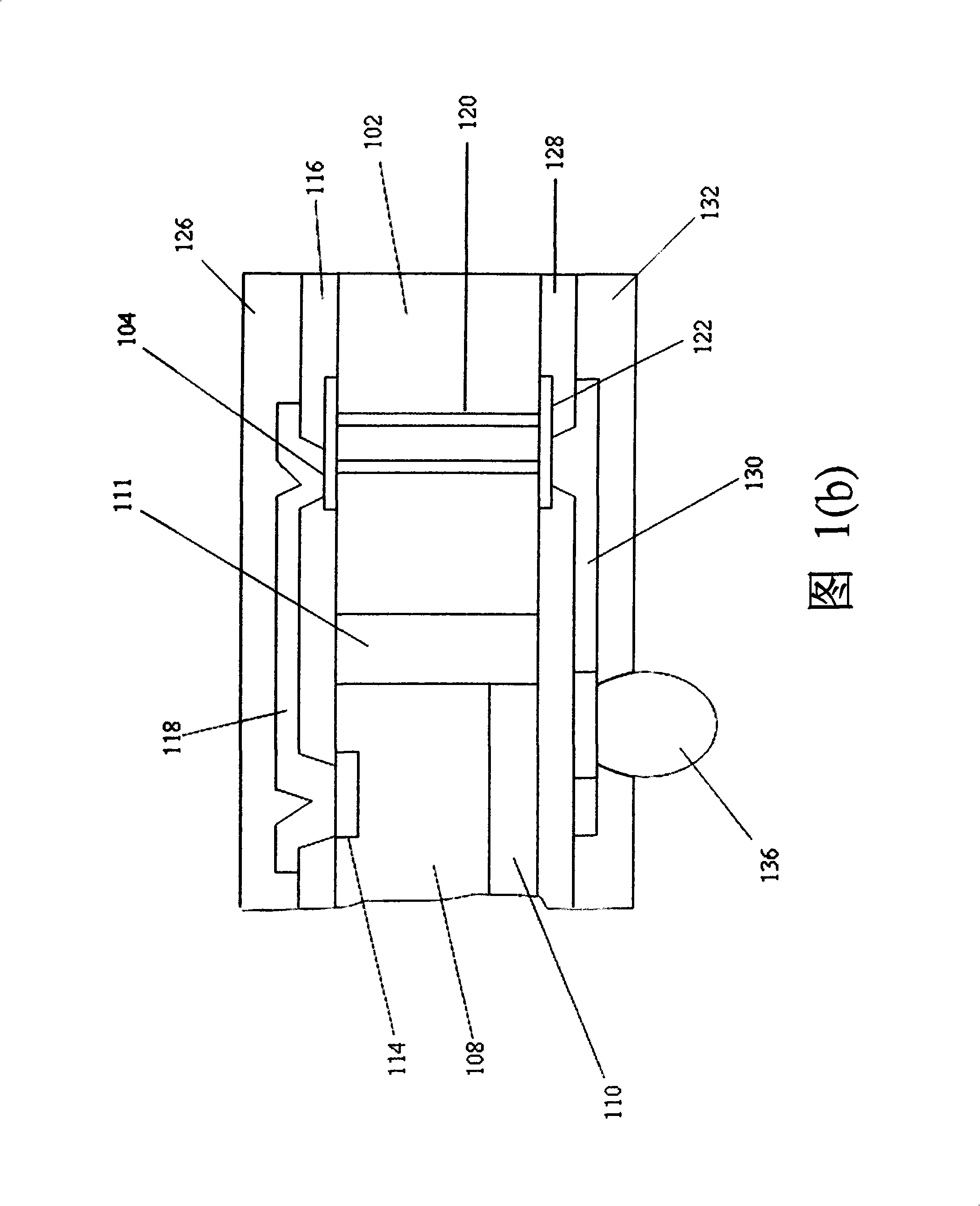
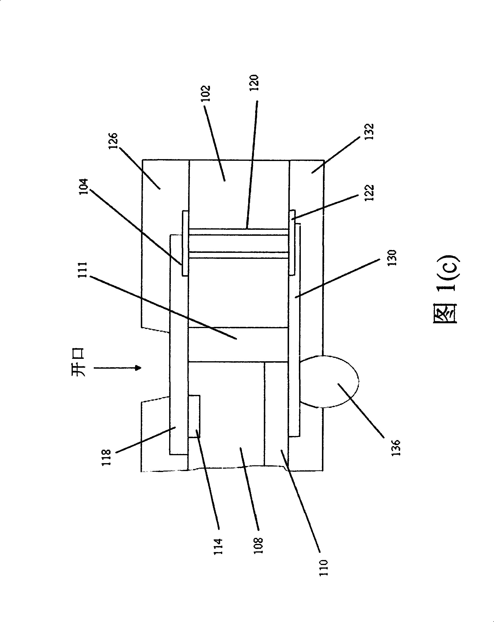
[0047] The present invention discloses a fan-out (or diffused) wafer-level packaging structure, using a substrate 102 which has a predetermined first terminal contact conductive pad 104 formed thereon, and pre-formed in the substrate 102 accommodating through-die holes 106 that will penetrate from the upper surface of the substrate to the lower surface of the substrate. At least one die with metal pads is disposed in the die-accommodating throug...
PUM
 Abstract
Description
Claims
Application Information
 - Generate Ideas
- Intellectual Property
- Life Sciences
- Materials
- Tech Scout
- Unparalleled Data Quality
- Higher Quality Content
- 60% Fewer Hallucinations
Browse by: Latest US Patents, China's latest patents, Technical Efficacy Thesaurus, Application Domain, Technology Topic, Popular Technical Reports.
© 2025 PatSnap. All rights reserved.Legal|Privacy policy|Modern Slavery Act Transparency Statement|Sitemap|About US| Contact US: help@patsnap.com