Supercharge Your Innovation With Domain-Expert AI Agents!

Method for forming micropatterns in semiconductor device

一种半导体、微图案的技术,应用在半导体/固态器件制造、电气元件、电路等方向

Inactive Publication Date: 2010-06-16
SK HYNIX INC
View PDF4 Cites 0 Cited by
  • Summary
  • Abstract
  • Description
  • Claims
  • Application Information

AI Technical Summary

Problems solved by technology

However, it is difficult to realize this new device due to technical limitations

Method used


Image

  • Method for forming micropatterns in semiconductor device
  • Method for forming micropatterns in semiconductor device
  • Method for forming micropatterns in semiconductor device

Examples


Embodiment Construction

[0016] Embodiments of the present invention relate to methods of forming micropatterns in semiconductor devices.

[0017] This embodiment will be described with reference to the drawings. In the drawings, exemplary thicknesses of layers and regions are exaggerated for ease of explanation. When a first layer is referred to as being "on" a second layer or "on" a substrate, it may mean that the first layer is formed directly on the second layer or on the substrate, or it may also mean that a third layer may be present on Between the first layer and the second layer or substrate. Furthermore, in different drawings, identical or similar reference numerals in different embodiments of the present invention indicate identical or similar elements.

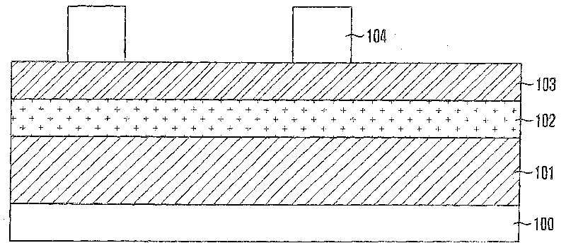
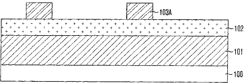
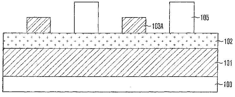
[0018] Figures 2A to 2J A cross-sectional view illustrating a method of forming a micropattern in a semiconductor device according to an embodiment of the present invention. In this embodiment, the hard mask formed on the gate electrod...


PUM


Abstract

A method for forming micropatterns in a semiconductor device includes forming a first etch stop layer over a etch target layer, forming a second etch stop layer over the first etch stop layer, forminga first sacrificial layer over the second etch stop layer, etching portions of the first sacrificial layer and second etch stop layer to form first sacrificial patterns, forming an insulation layer along an upper surface of the first etch stop layer, forming a second sacrificial layer over the insulation layer to cover the insulation layer, planarizing the second sacrificial layer and the insulation layer to expose the first sacrificial patterns, removing the first sacrificial patterns and the second sacrificial layer, etching the second etch stop layer and insulation layer to thereby form second sacrificial patterns, etching the first etch stop layer, and etching the etch target layer.

Description

[0001] related application [0002] This application claims priority from Korean Patent Application No. 2007-0092642 filed on September 12, 2007, the entire contents of which are incorporated herein by reference. technical field [0003] The present invention relates to methods of fabricating micropatterns in semiconductor devices. Background technique [0004] Recently, as semiconductors become highly integrated, lines and spaces (LS) below 40 nm are required. However, typical exposure equipment cannot form LSs below 60 nm. Therefore, a double patterning technique (DPT) has been introduced to form fine LSs below 60 nm using typical exposure equipment. [0005] Figures 1A to 1D A cross-sectional view illustrating a method of forming a typical micropattern by a DPT process is illustrated. refer to Figure 1A , forming an etching target layer 101 on the substrate 100 . First and second hard masks 102, 103 are sequentially formed on the resulting structure. [0006] A ph...

Claims


Application Information

Patent Timeline
Patent Type & Authority Patents(China)
IPC IPC(8): H01L21/00H01L21/02H01L21/033
CPCH01L21/31144H01L21/32139H01L21/0337H01L21/0338H01L21/32
Inventor 金原圭李基领
Owner SK HYNIX INC
Features
  • R&D
  • Intellectual Property
  • Life Sciences
  • Materials
  • Tech Scout
  • Unparalleled Data Quality
  • Higher Quality Content
  • 60% Fewer Hallucinations
Learn More