

Processing method of brittle material substrate
A technology of brittle material substrates and processing methods, applied in stone processing equipment, metal processing equipment, fine working devices, etc., can solve problems such as insufficient crack position control
- Summary
- Abstract
- Description
- Claims
- Application Information
AI Technical Summary
Problems solved by technology
Method used
Image

Examples
Embodiment Construction
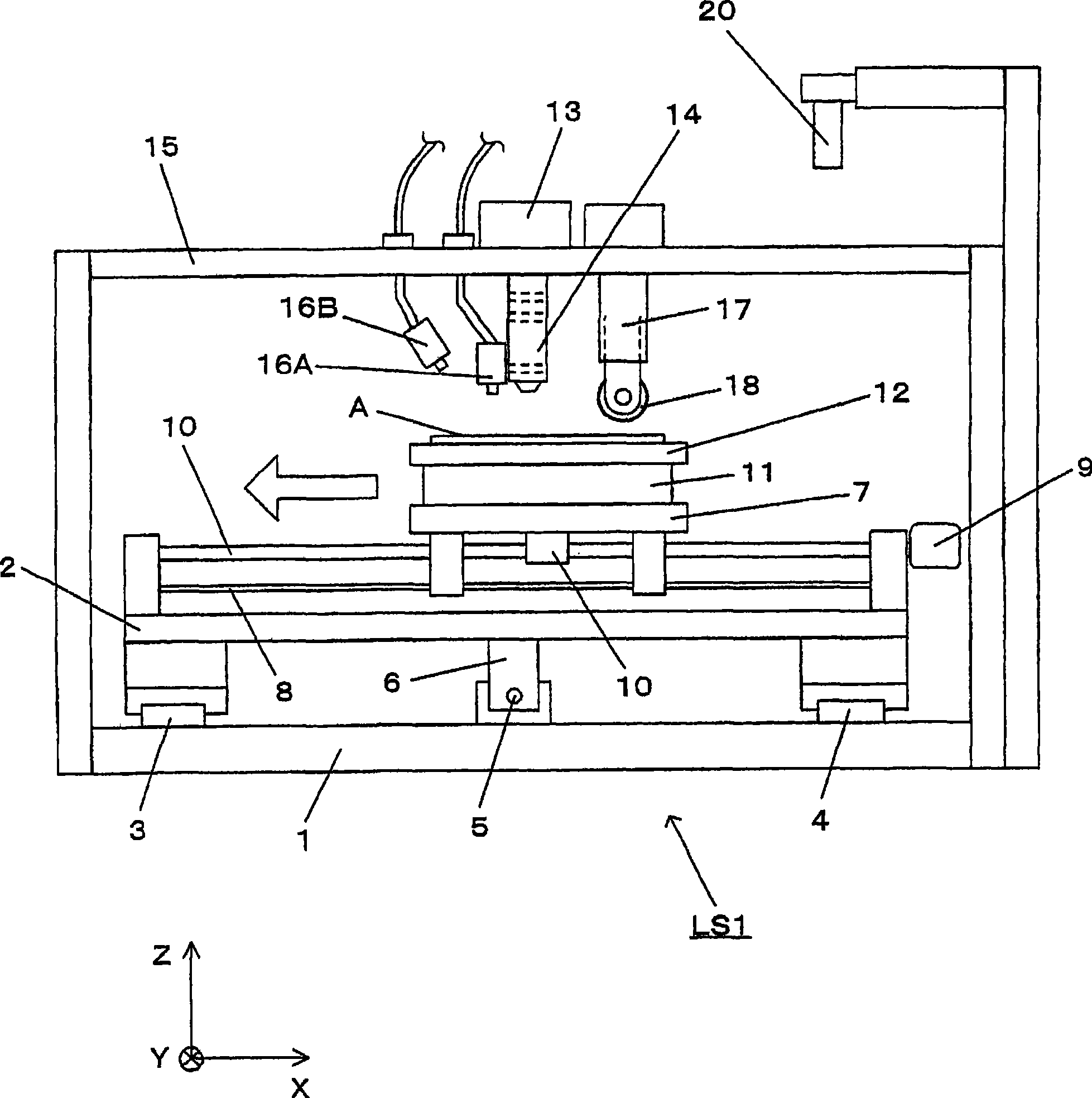
[0049] Embodiments of the present invention will be described below based on the drawings. figure 1 It is a structural schematic diagram of the substrate processing apparatus LS1 which is one embodiment of this invention. Here, the case of processing a glass substrate will be described as an example.
[0050] First, the overall configuration of the substrate processing apparatus LS1 will be described. The substrate processing apparatus LS1 is provided with a slide table 2 that is positioned along a pair of guide rails 3 and 4 arranged in parallel on the horizontal stage 1. figure 1 The front and rear direction of the paper (hereinafter referred to as the Y direction) reciprocates. A lead screw (skullu-neji) 5 is arranged between the two guide rails 3, 4 along the front-rear direction, and the strut 6 fixed on the above-mentioned sliding table 2 is screwed on the lead screw 5, and is driven by a motor (not shown). (shown) make the lead screw 5 forward and reverse, and the sl...
PUM
 Abstract
Description
Claims
Application Information