Planar array exposure device and exposure method thereof

A technology of exposure device and exposure method, which is applied in the direction of developing and printing devices, optics, instruments, etc., can solve the problems of affecting the exposure efficiency, affecting the exposure speed, and taking a long time, so as to improve the exposure efficiency, increase the exposure speed, and reduce the positioning time Effect

Inactive Publication Date: 2010-08-25
HANS LASER TECH IND GRP CO LTD +1
View PDF0 Cites 0 Cited by
  • Summary
  • Abstract
  • Description
  • Claims
  • Application Information

AI Technical Summary

Problems solved by technology

[0004] The disadvantage of the existing technology is that the movement of the exposure head along the X direction needs to reach the predetermined position every time, but due to the accuracy of the equipment and the problems of acceleration and deceleration in the movement, the exposure head generally stops near the predetermined position , and then the position of the exposure head must be oscillatingly adjusted through the feedback information of the servo system until it is adjusted to the accurate predetermined position before exposure can be started. This process takes a long time
This also indirectly affects the entire exposure speed and exposure efficiency

Method used


Image

  • Planar array exposure device and exposure method thereof
  • Planar array exposure device and exposure method thereof
  • Planar array exposure device and exposure method thereof

Examples


Embodiment Construction

[0029] The present invention will be further described in detail below through specific embodiments and in conjunction with the accompanying drawings.

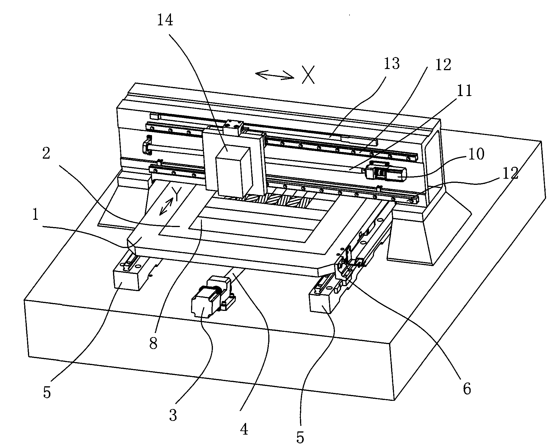
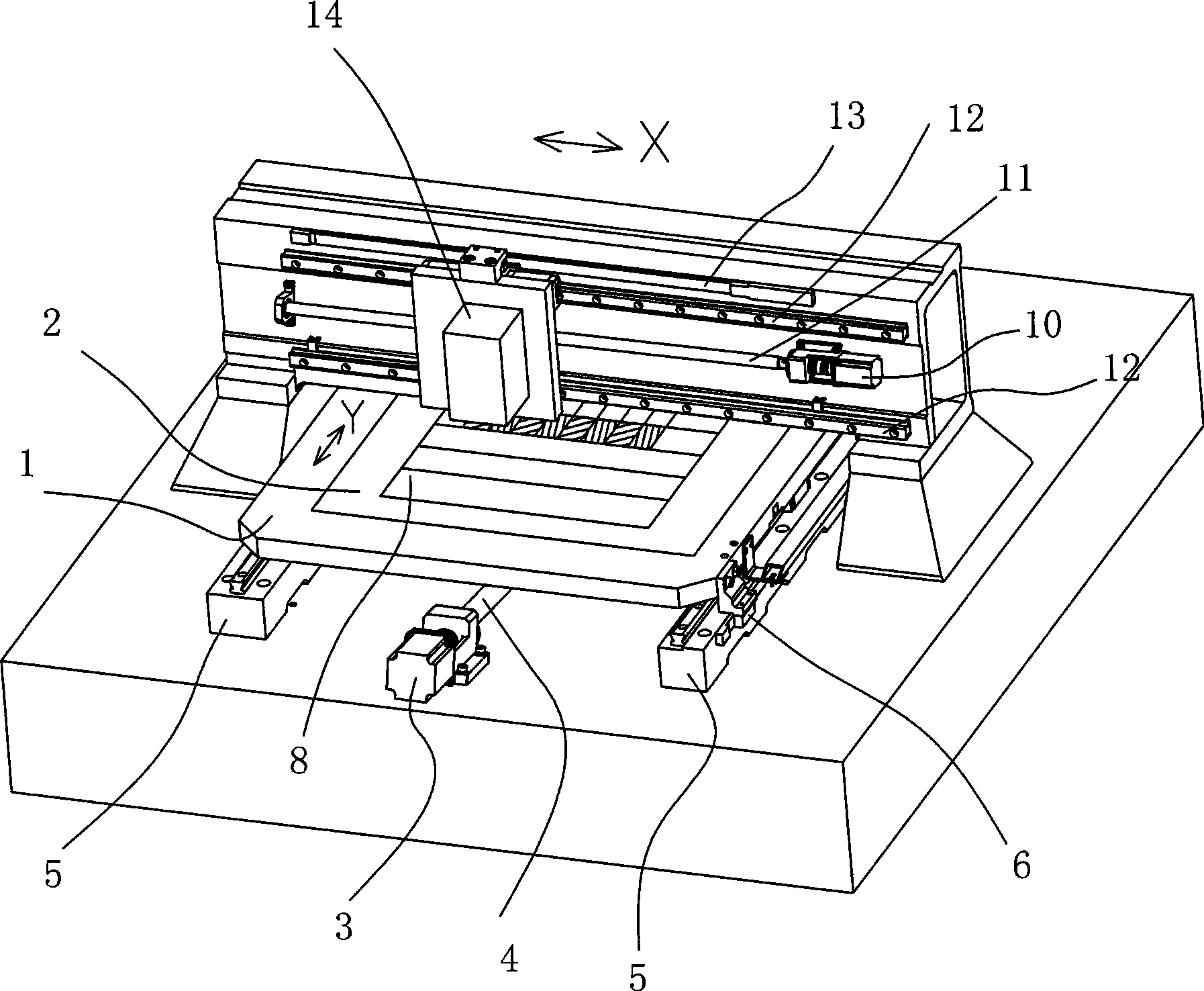
[0030] The invention relates to an area array exposure device and an exposure method for performing digital exposure on a photosensitive surface. The invention is especially suitable for the field of computer plate making and the field of photographing.

[0031] As shown in FIG. 2 , an area array exposure device includes: a memory (not shown in the figure), an exposure head 14 , a movement unit, a sensor 13 , and a controller (not shown in the figure). The image to be exposed is stored in the memory. The movement unit drives the exposure head 14 to move from the Nth (N is a positive integer) exposure position to the vicinity of the adjacent N+1th preset exposure position. The sensor 13 detects the stop position of the exposure head 14 and outputs it to the controller. The controller judges whether the stop position of the ex...


PUM


Abstract

The invention discloses an area array exposure device and an exposure method. The method comprises the following steps: a moving step in which an optical head of the area array exposure device moves to a position near an adjacent N+1st preset exposure position after exposing an Nth image block at an Nth exposure position, wherein N is a positive integer; a detection and adjustment step in which aposition at which the optical head stops is detected to judge whether complete pixel splicing can be realized among adjacent image blocks, if yes, an exposure step is carried out, if no, the positionof the optical head is adjusted finely to realize the complete pixel splicing of the adjacent image blocks and then turn to the exposure step; an exposure step in which the N+1st image block is exposed at the N+1st actual exposure position, and a starting point of the N+1st image block is connected with an end point of the Nth image block; and the steps are repeated until the image to be exposed is completely exposed. In the method, the position adjustment range of the optical head is controlled within the width of the pixels, thus largely reducing the positioning time and improving the exposure efficiency.

Description

technical field [0001] The invention relates to an area array exposure device, and also relates to an exposure method of the area array exposure device. Background technique [0002] As shown in Figure 1, the exposure method of the existing area array exposure device is as follows: the image splitter divides the image data 21 to be exposed into small block-shaped partial images such as 30 according to the maximum area and resolution of the exposure of the exposure head. , 31, the length d of the partial images in the X direction shown in the figure is basically the same, and the image data to be exposed are stored in the memory in the form of small block partial image data. [0003] At a predetermined exposure position, the light modulator in the exposure head takes out partial image data such as 30 from the memory, and spatially modulates the light beam emitted from the light source. ), the light beam reflected by the DMD is irradiated to the imaging surface through the le...

Claims


Application Information

Patent Timeline
Patent Type & Authority Patents(China)
IPC IPC(8): G03B27/32G03B27/52G03B27/72
Inventor 高云峰孙海翔
Owner HANS LASER TECH IND GRP CO LTD
Why Eureka
Try Eureka