Silicon substrate having flip chip projection

A flip-chip and silicon technology, applied in electrical components, electrical solid devices, circuits, etc., can solve problems affecting the wavelength of the emission light source, difficulty in batch production, size and heat dissipation efficiency limitations, etc., to increase optical effects and simplify The effect of component complexity

Inactive Publication Date: 2012-02-29
WALSIN LIHWA
View PDF0 Cites 0 Cited by
  • Summary
  • Abstract
  • Description
  • Claims
  • Application Information

AI Technical Summary

Problems solved by technology

[0005] Since the known light emitting diode packaging structure 10 needs to form the cup-shaped base 12 first, complete the packaging by molding or potting, and then integrate the individual light emitting diode packaging structures 10 on the printed circuit board 24 by surface mounting technology, the process is complicated. Difficult to mass produce
When applied to a high-power light-emitting diode packaging structure 10, the cup-shaped substrate 12 used to carry the photoelectric element 16 will affect the wavelength of the emitted light source, brightness attenuation, and even cause problems such as element burnout due to overheating.
Due to the bulky volume of the known LED packaging structure 10 and the heat dissipation requirements of the high-power LED packaging structure 10, the size and heat dissipation efficiency of the entire LED packaging structure 10 are limited.

Method used


Image

  • Silicon substrate having flip chip projection
  • Silicon substrate having flip chip projection
  • Silicon substrate having flip chip projection

Examples


Embodiment Construction

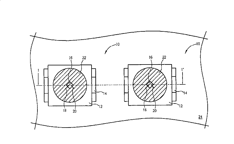
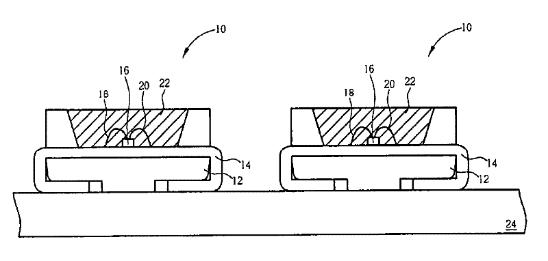
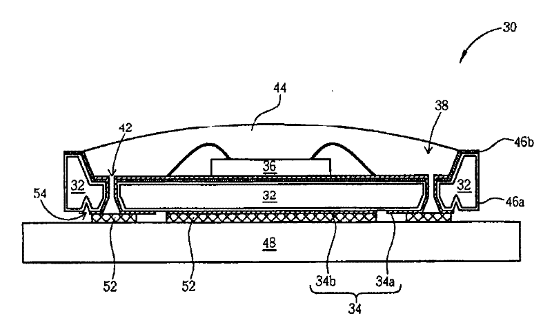
[0066] Please refer to image 3 and Figure 4 , image 3 is a schematic cross-sectional view of a photoelectric element packaging structure with a silicon substrate according to the first preferred embodiment of the present invention, and Figure 4 for image 3 The schematic top view of the package structure of the optoelectronic element shown. It should be noted that the drawings are for illustration purposes only and are not drawn to original scale. Such as image 3 and Figure 4 As shown, the photoelectric device packaging structure 30 includes a silicon substrate 32 , a plurality of guiding wires 34 and at least one photoelectric device 36 . The material of the silicon substrate 32 includes polysilicon, amorphous silicon or single crystal silicon, can be a square silicon chip or a circular silicon chip, and can contain integrated circuits or passive components therein. The silicon substrate 32 has an upper surface and a lower surface, and a concave cup structure 38 ...


PUM


Abstract

The invention provides a siliceous base plate with a flip clip lug. The lot manufacturing of the siliceous base plate is conducted by utilizing the micro electromechanical process or the semiconductor process so as to manufacture the diversified and precise siliceous base plate. According to the property of the siliceous base plate and the arrangement of a guiding connection line, a photoelectricelement, a concave structure and a flip chip lug and other elements on the siliceous base plate, the invention can increase the optical effect and the radiating effect of the encapsulating structure of the photoelectric element as well as the reliability of the encapsulating structure, and simplifies the element complexity of the encapsulating structure of the photoelectric element.

Description

[0001] This application is a divisional application of Chinese Patent Application No. 200610100967.2 with a filing date of August 4, 2006 and an invention title of "Silicon Substrate and Photoelectric Component Encapsulation Structure with Silicon Substrate". technical field [0002] The invention relates to a silicon substrate with flip-chip bumps, in particular to a photoelectric element packaging structure with a silicon substrate manufactured by micro-electromechanical technology or semiconductor technology. Background technique [0003] Light-emitting diode (light-emitting diode; LED) components belong to cold light, which has the advantages of low power consumption, long component life, no need to warm up the lamp time, and fast response speed. It is easy to make extremely small or array elements according to application requirements, so light-emitting diode elements have been widely used in indicator lights and display devices of information, communication, and consume...

Claims


Application Information

Patent Timeline
Patent Type & Authority Patents(China)
IPC IPC(8): H01L23/492H01L23/34
CPCH01L2224/48091
Inventor 林弘毅
Owner WALSIN LIHWA
Why Eureka
Try Eureka