Wafer detection system

A detection system and wafer technology, applied in the direction of measurement devices, electronic circuit testing, semiconductor/solid-state device testing/measurement, etc., can solve problems affecting the overall production capacity output, incompatibility, inaccurate detection results, etc., to improve the detection process speed effect

Active Publication Date: 2009-05-13
YOUNGTEK ELECTRONICS
View PDF0 Cites 32 Cited by
  • Summary
  • Abstract
  • Description
  • Claims
  • Application Information

AI Technical Summary

Problems solved by technology

[0005] However, in the existing process, the result of manual inspection cannot be traced back to the result of electrical measurement, so there is a great incompatibility between the two in terms of coordination and connection, which makes the time schedule of manual inspection affect the overall production capacity output, which is more likely to cause inaccurate detection results

Method used


Image

  • Wafer detection system
  • Wafer detection system
  • Wafer detection system

Examples


Embodiment Construction

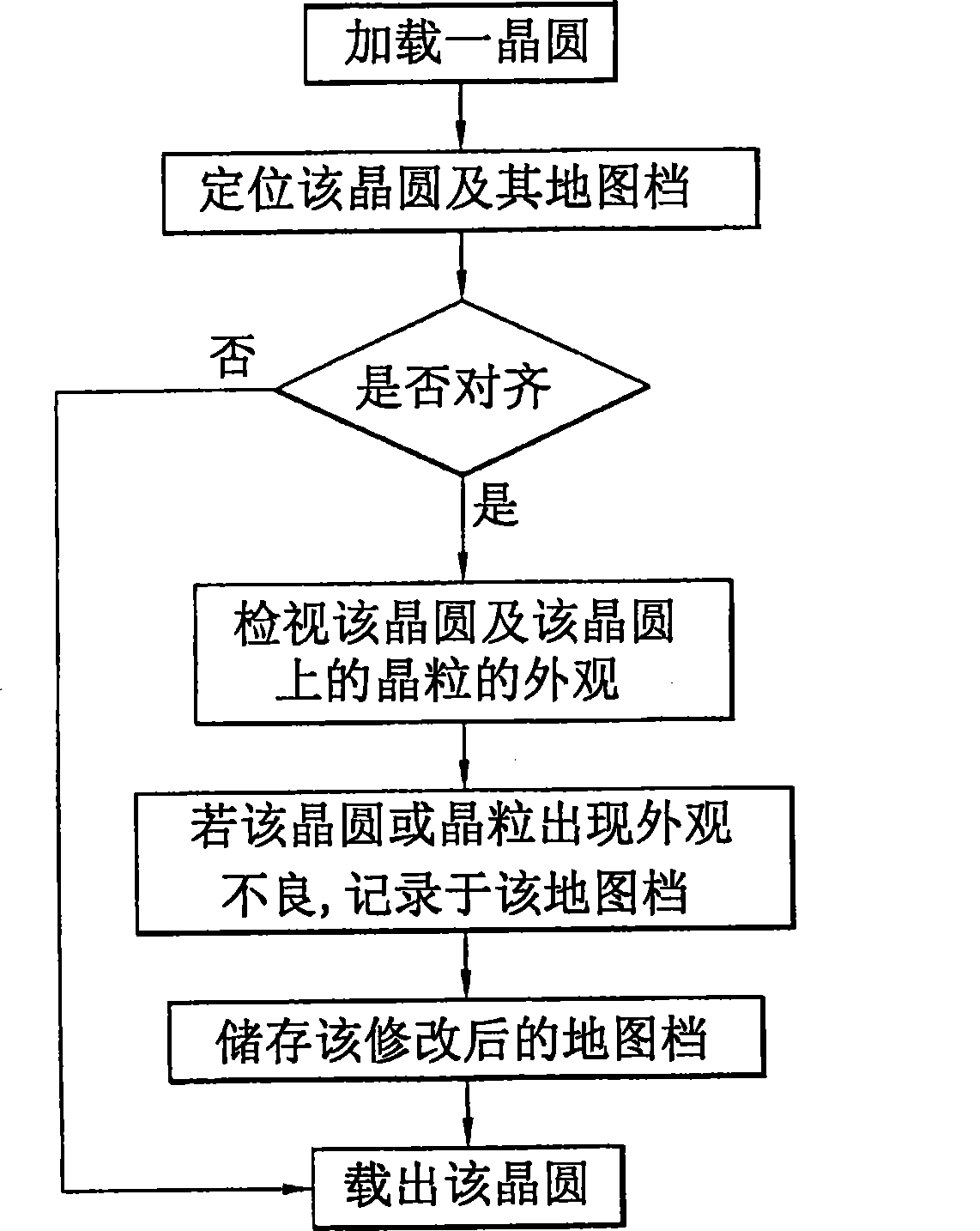
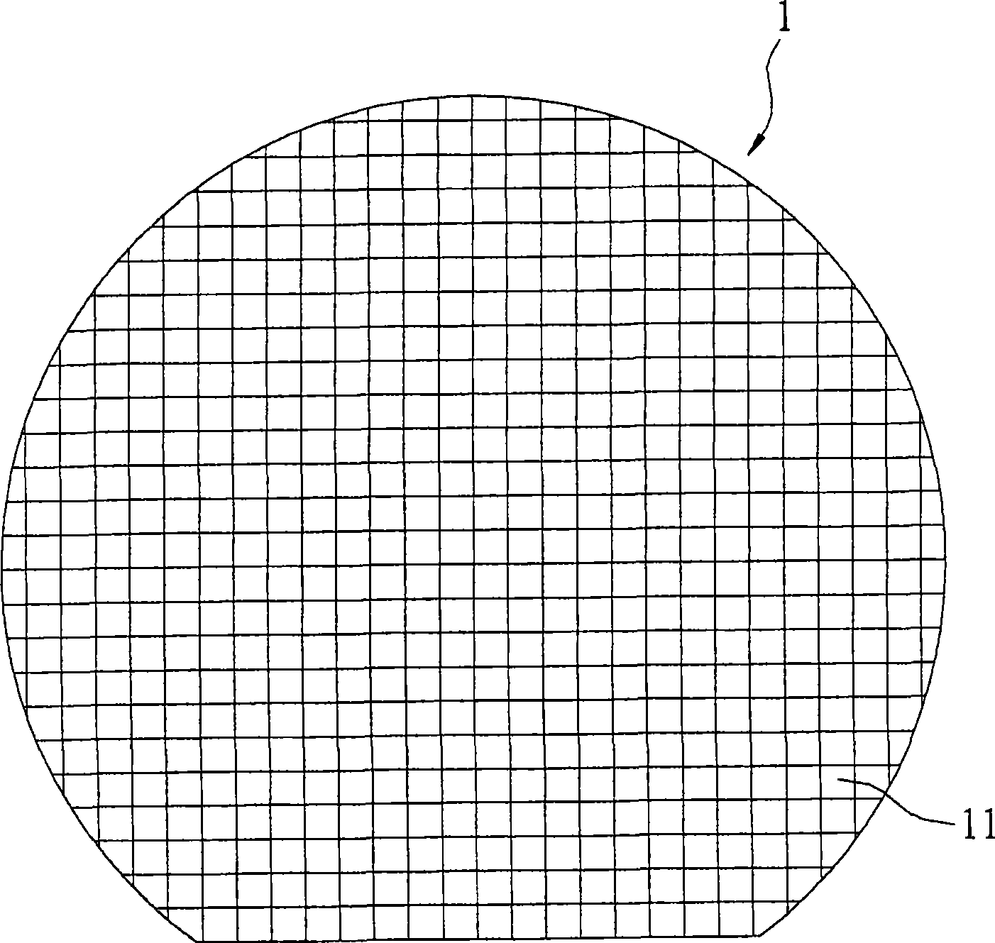
[0025] After the final process on the production line, the wafer must be diced into individual dies for packaging. However, before packaging, it is necessary to check whether the electrical function of each chip is normal, that is, use an electrical measurement probe to detect whether the electrical function of each chip is normal, and use the result of the test as a The electronic map file is output, usually the map file is in a special file format, and in this embodiment, the file format is the first file format. The existing manual inspection cannot be done in a computerized way, so the operator must first record in paper. However, in the present invention, the operation of manual inspection is applied to a production platform, so that it can directly read the electronic map file, and directly record the result of visual inspection in the map file.

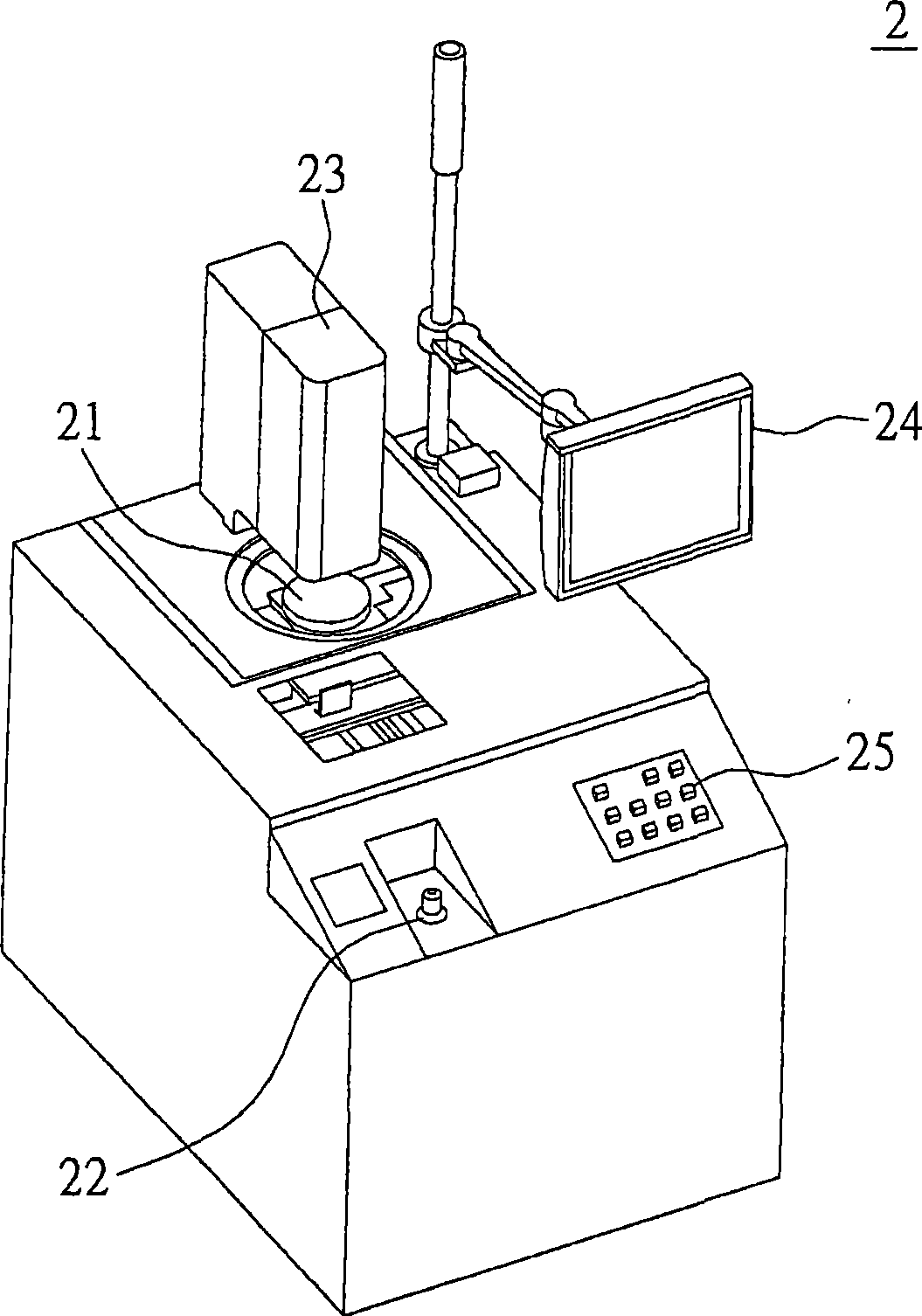
[0026] see figure 2 , the present invention provides a wafer inspection system 2, the wafer inspection system 2 is mainly ...


PUM


Abstract

The invention relates to a wafer detection system comprising the following steps: loading a wafer and positioning the wafer with a map file corresponding to the wafer, wherein, the map file is of a first file format; examining the appearance of the wafer; recording and correcting the data of the map file if the appearance of the wafer is not good; and storing the corrected map file. Thereby, direct correction and marking of the map file can be carried out, and detection time can be effectively saved.

Description

technical field [0001] The invention relates to a wafer detection system, in particular to a wafer detection system which directly modifies map files to improve detection efficiency. Background technique [0002] With the gradual application of electronic concepts such as personal mobile information, e-commerce, global communication, and digital home in modern life, the semiconductor manufacturing industry is growing rapidly in response to the needs of various applications. In contrast, the increase in production capacity and yield rate in the semiconductor manufacturing process also improves the development of the semiconductor industry. [0003] Generally speaking, in order to implement circuit functions on a semiconductor substrate, the semiconductor substrate must go through the following steps, such as deposition of metal layers, patterning on each layer of material by yellow light process, ion implantation and other related processes. In order to ensure that the resul...

Claims


Application Information

Patent Timeline
Patent Type & Authority Applications(China)
IPC IPC(8): H01L21/66G01N21/956G01R31/28
Inventor 汪秉龙陈信呈周明澔
Owner YOUNGTEK ELECTRONICS
Why Eureka
Try Eureka