Method for manufacturing antenna element and antenna module with the same

A technology of antenna elements and antenna modules, which is applied to antenna components, antennas, folding antennas, etc., can solve the problems of difficult programming of laser processing and prolonged laser processing time, and achieve the best assembly convenience and reworkability. Time-saving, easy-to-adjust or transform effects

Active Publication Date: 2009-05-20
WISTRON NEWEB
View PDF0 Cites 2 Cited by
  • Summary
  • Abstract
  • Description
  • Claims
  • Application Information

AI Technical Summary

Problems solved by technology

[0004] However, since the outer shell structure of each electronic device is different, the design of the conductive circuit is more likely to be limited by the outer structure of the electronic device shell, and when laser processing is performed, if the desired processing On the shell, when the conductive lines are distributed in a wide area and not concentrated, the entire laser processing time will also be lengthened. In addition, the structure of the shell and the position of the conductive lines in the shell will also affect the laser processing program. difficulty on

Method used


Image

  • Method for manufacturing antenna element and antenna module with the same
  • Method for manufacturing antenna element and antenna module with the same
  • Method for manufacturing antenna element and antenna module with the same

Examples


Embodiment Construction

[0057] The aforementioned and other technical contents, features and effects of the present invention will be clearly presented in the following detailed description of two preferred embodiments with reference to the accompanying drawings.

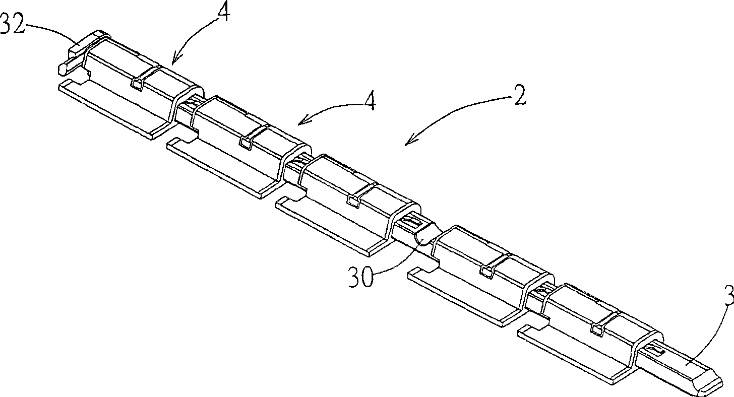
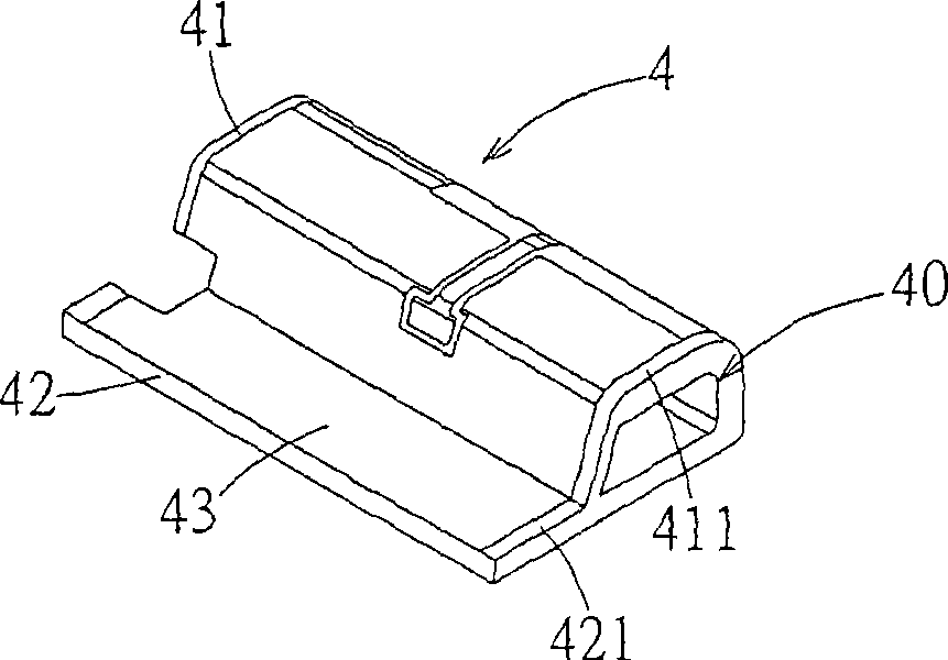
[0058] refer to Figure 1 ~ Figure 3 The first preferred embodiment of the MID antenna module 2 of the present invention includes an antenna frame 3 and a plurality of antenna elements 4 arranged on the antenna frame 3, and the MID antenna module 2 can be arranged on a notebook computer (such as Figure 6 shown) or other portable communication electronic devices to be used as the antenna of the electronic device.

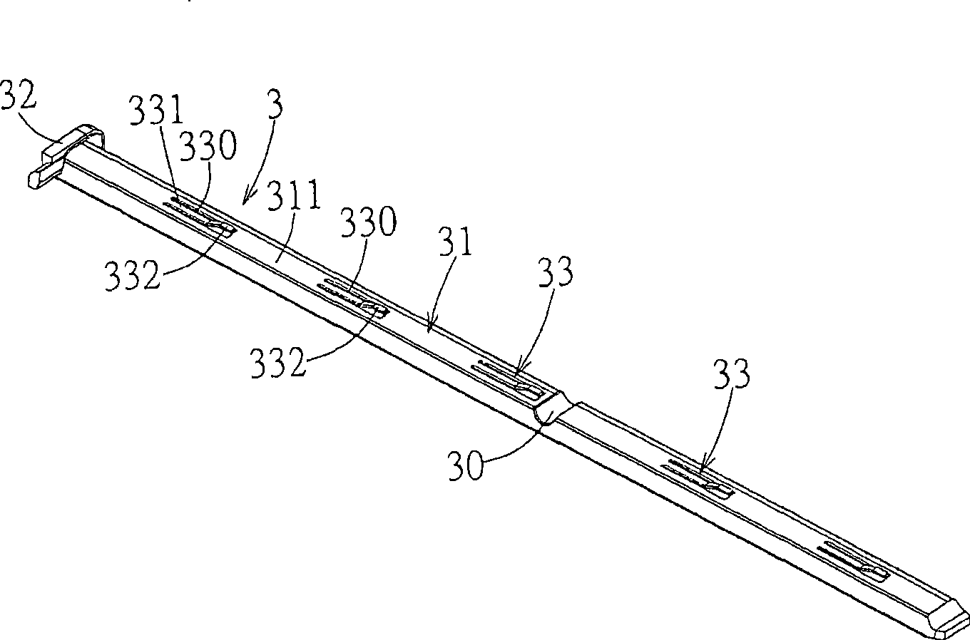
[0059] Such as figure 2As shown, the antenna frame 3 includes a generally elongated frame body 31 , a wire fixing portion 32 disposed on the frame body 31 , and a plurality of first limiting members 33 . The frame body 31 is strip-shaped and has a top wall 311 , and the frame body 31 is made of plastic material. The wire fix...


PUM


Abstract

The invention discloses a method for manufacturing an MID antenna element and an MID antenna module with the MID antenna element. The MID antenna module comprises an antenna mount and a plurality of antenna elements which are glidingly connected to the antenna mount, each antenna element is provided with a body and a conducting wire arranged in the body, the conducting wires of the antenna elements are formed by serially connecting the bodies and arranging the bodies in a laser processing mode, and can be a specification type used for different transmission applications, and the antenna elements are serially connected into a modular MID antenna by means of the antenna mount and are arranged on wireless communication electronic devices such as a notebook computer or a mobile phone and so on, thereby overcoming the defect that in the prior MID technology, wires of an antenna are directly arranged on a shell of an electronic device to make the arrangement and processing of the antenna easier to be limited by a shell structure of the electronic device.

Description

technical field [0001] The present invention relates to an antenna, and more particularly to a modular molded interconnect circuit assembly antenna. Background technique [0002] Most of the existing methods for built-in antennas in mobile phones are to fix the metal sheet on the back shell of the mobile phone in a plastic hot-melt manner, or directly attach the metal sheet to the back shell of the mobile phone. This current method has many constraints, including complex manufacturing process, many parts, high cost, and long assembly time. In order to improve the above manufacturing shortcomings, the 3D-MID technology that can be used in small mobile electronic devices has been developed. [0003] The so-called 3D-MID (Three Dimensional Mold Inter-connection Device, three-dimensional circuit board injection molding engineering, or three-dimensional molded interconnection circuit components) technology refers to the process of laser processing (LDS) directly on the injection...

Claims


Application Information

Patent Timeline
IPC IPC(8): H01Q1/00H01Q1/08H01Q1/12H01Q1/22H01Q1/38H05K3/02
Inventor 罗文魁陈恒安
Owner WISTRON NEWEB
Why Eureka
Try Eureka