

A method for making nanoscale graphics
A nanoscale, graphic technology, applied in the direction of manufacturing microstructure devices, photolithographic process of patterned surface, process for producing decorative surface effects, etc., can solve the problems of focused electron beam affecting resolution and high cost, and achieve high resolution, resolution of high cost, low cost effects
- Summary
- Abstract
- Description
- Claims
- Application Information
AI Technical Summary
Problems solved by technology
Method used
Image

Examples
Embodiment Construction
[0026] In order to make the object, technical solution and advantages of the present invention clearer, the present invention will be described in further detail below in conjunction with specific embodiments and with reference to the accompanying drawings.
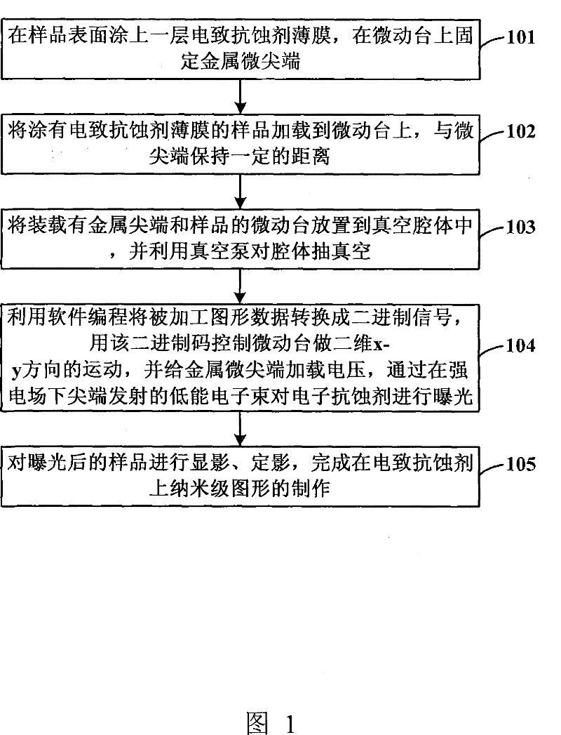
[0027] Such as figure 1 as shown, figure 1 It is a flow chart of the method for making nanoscale graphics using electron beams generated by field emission provided by the present invention. The nanoscale graphics convert graphic data into binary signals to control the two-dimensional x-y direction movement of the micro-motion stage and the loading of the metal tip voltage , obtained by exposing the electronic resist with an electron beam generated after the tip is loaded with a voltage, the method includes:
[0028] Step 101: Coating a layer of electroresist film on the surface of the sample, and fixing the metal microtip on the micro-motion stage; in this step, a layer of electroresist is coated on the surface of the sa...
PUM
 Abstract
Description
Claims
Application Information