Grounding loop structure of radio frequency CMOS integration inductance
A technology that integrates inductors and grounding rings. It is applied to circuits, electrical components, and electric solid devices to prevent magnetic energy loss and ensure the Q value of inductors.
- Summary
- Abstract
- Description
- Claims
- Application Information
AI Technical Summary
Problems solved by technology
Method used
Image

Examples
Embodiment Construction
[0013] The present invention will be described in further detail below in conjunction with the accompanying drawings and embodiments.
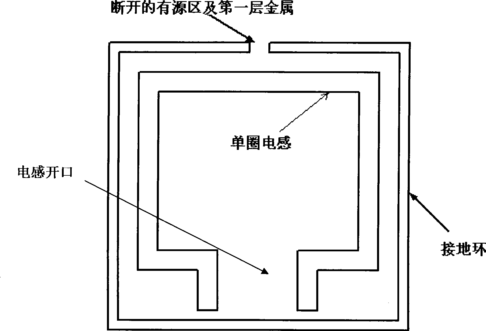
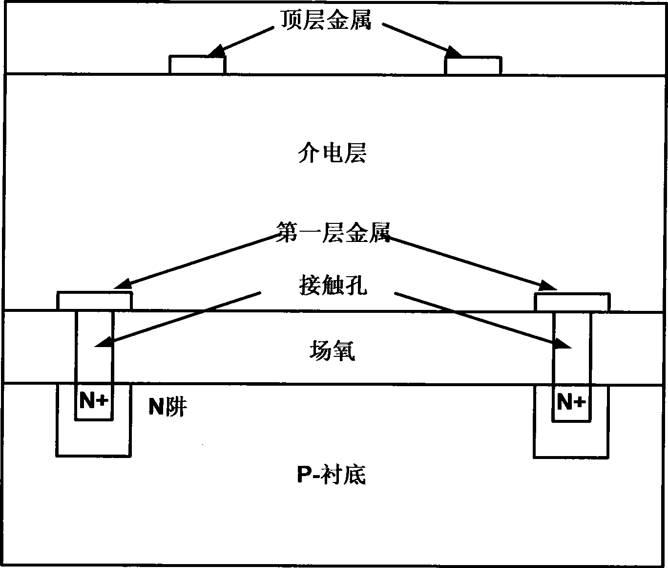
[0014] like figure 1 As shown, the present invention proposes a ground ring structure in a novel RF CMOS integrated inductor, that is, by disconnecting the active area of the ground ring and its upper wiring metal (Metall, that is, the first layer of metal), so that a closed loop cannot be formed around the inductor. The loop is used to reduce the loss of magnetic field energy on the ground ring and avoid a significant drop in the Q value.
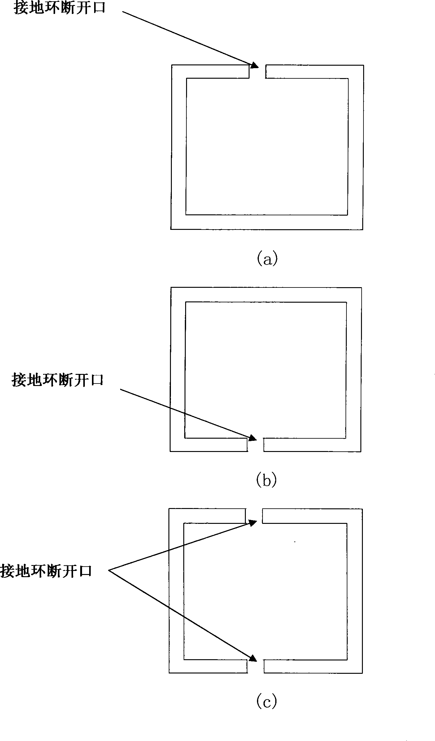
[0015] like image 3 As shown, the grounding ring structure in a radio frequency CMOS integrated inductor of the present invention, the opening of the grounding ring (that is, the opening of the grounding ring active area and the opening of the first layer of metal) and the direction of the opening of the inductor can be the same or opposite, E.g, image 3 (a) The opening of the ground ring and the op...
PUM
 Abstract
Description
Claims
Application Information
 - R&D
- Intellectual Property
- Life Sciences
- Materials
- Tech Scout
- Unparalleled Data Quality
- Higher Quality Content
- 60% Fewer Hallucinations
Browse by: Latest US Patents, China's latest patents, Technical Efficacy Thesaurus, Application Domain, Technology Topic, Popular Technical Reports.
© 2025 PatSnap. All rights reserved.Legal|Privacy policy|Modern Slavery Act Transparency Statement|Sitemap|About US| Contact US: help@patsnap.com