Waveform antialiasing method and waveform antialiasing processing apparatus

A processing device and anti-aliasing technology, which is applied to cathode ray tube indicators, instruments, static indicators, etc., can solve problems such as limiting the scope of use, and achieve the effect of continuous and smooth waveform display and optimized waveform display effect

Inactive Publication Date: 2009-06-17
SHENZHEN MINDRAY BIO MEDICAL ELECTRONICS CO LTD
View PDF0 Cites 11 Cited by
  • Summary
  • Abstract
  • Description
  • Claims
  • Application Information

AI Technical Summary

Problems solved by technology

[0006] The defects of the above two methods limit the range of application of the existing technical solutions, making them generally used for anti-aliasing of still images, characters and curves, and not suitable for processing real-time waveforms

Method used


Image

  • Waveform antialiasing method and waveform antialiasing processing apparatus
  • Waveform antialiasing method and waveform antialiasing processing apparatus
  • Waveform antialiasing method and waveform antialiasing processing apparatus

Examples


Embodiment 1

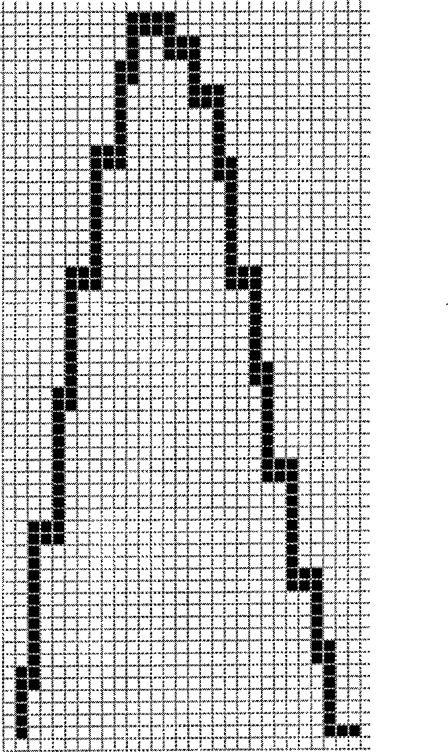
[0038] like figure 2 , image 3 and Figure 4 , Figure 13 As shown, first, the sampling unit samples three consecutive sampling points to obtain three sets of adjacent data of the previous sampling point, the current sampling point, and the next sampling point. The data sampled by each sampling point corresponds to a column of pixels, and the areas where the three columns of pixels are located are respectively limited by their upper and lower boundary values. Assume that the areas corresponding to the three groups of adjacent data pixels are (min a-1 , max a-1 ), (min a , max a ) and (min a+1 , max a+1 ); the calculation unit determines to process the current sampling point according to the above-mentioned three groups of data, that is, the waveform line segment sampled by the second sampling point, and the processing area is the area between the maximum value and the minimum value of the three groups of data, i.e. (min(min a-1 , min a , min a+1 ), max(max a-1 , m...

Embodiment 2

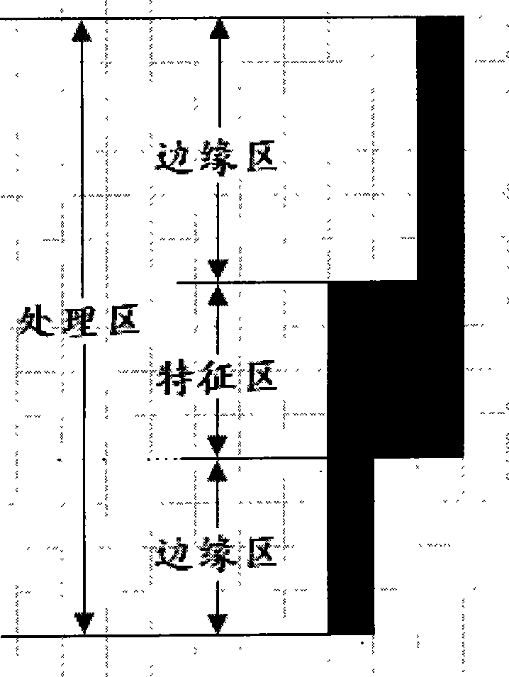
[0044] like Figure 5 , Image 6 and Figure 7 As shown, the difference with Embodiment 1 is that the graphic sampled by the current sampling point is longer; for this embodiment, the processing area is (min a , max a ), the feature area is the public area (min a-1 , max a+1 ), the edge area is the area except the feature area in the processing area, including (min a , min a-1 ) and (max a+1 , max a ) in two parts. Fill the foreground color in the feature area, and fill the transition color between the foreground color and the background color in the edge area. The color filling of the pixels in the edge area is the same as the method in Embodiment 1, Figure 7 is true Figure 5 The second sampling point in is the anti-aliased result of the waveform of the current sampling point.

Embodiment 3

[0046] like Figure 8 , Figure 9 and Figure 10 As shown, the difference from Embodiment 1 and Embodiment 2 is that there is no common intersection of extreme values ​​of three consecutive sampling points, min a =min at and max a =max at ; In this case, the processing area of ​​the waveform line segment of the second sampling point is still the collection of extreme values ​​of the three sampling points, in this case (min a , max a ); the characteristic area is the unique area of ​​the extreme value of the waveform of the current sampling point, that is, the blank area of ​​the two sets of data before and after the first and third sampling point (max a+1 , min a-1 ); the edge area is the area outside the feature area in the processing area, that is (min a , max a+1 ) and (min a-1 , max a ). Fill the foreground color in the feature area, and fill the transition color between the foreground color and the background color in the edge area. The color filling of pixel...


PUM


Abstract

The invention discloses a waveform saw tooth resisting method and a waveform saw tooth resistance processing device. The treatment on the displayed waveform line of prior sampling points comprises: using a sampling unit to obtain three data groups of adjacent domains of the displayed waveform lines of the last sampling point, the prior sampling point and the next sampling points; according to the data of adjacent domains, using a calculation unit to determine the characteristic region and the marginal region of the displayed waveform line of the prior sampling point; using a display processing unit to display the characteristic region via foreground color and display the marginal region via graded color. The invention can effectively resolve the saw tooth condition of waveform, and only needs to obtain the data of the prior sampling point, the last sampling point and the next sampling point to processing the image of one sampling period, to process saw tooth resistance. The method has low computational amount and no delay, is especially suitable for processing real-time waveform, and processing the waveform of small size and insufficient data of adjacent domains.

Description

technical field [0001] The invention relates to a waveform processing method and processing device, in particular to a method and device for performing anti-aliasing on waveforms. Background technique [0002] Sampling and displaying waveforms are involved in many fields. From a mathematical point of view, the waveform is a continuous smooth curve, and all its points are infinitely small "ideal" points; but the display is not an "ideal" display medium, it is discrete, the smallest The display unit of the display is a pixel; a pixel is not a point, but a tiny rectangular area on the screen; this difference leads to almost all waveforms, whose data points are not always exactly one-to-one corresponding to the pixels on the display, except for this waveform When it is vertical, horizontal or inclined at 45 degrees, but such waveforms are rare. The simplest and fastest method is to discard the data that cannot be corresponded, and connect the points that can be accurately corr...

Claims


Application Information

Patent Timeline
Patent Type & Authority Applications(China)
IPC IPC(8): G09G5/00G09G5/02
Inventor 陶华刘帅军
Owner SHENZHEN MINDRAY BIO MEDICAL ELECTRONICS CO LTD
Why Eureka
Try Eureka