Semiconductor device, display device and electronic device

A semiconductor and display technology, applied in the fields of semiconductor devices, semiconductor/solid-state device manufacturing, semiconductor/solid-state device components, etc., to achieve the effects of improving reliability, good traceability, and simplifying quality management

Inactive Publication Date: 2009-09-09
SHARP KK
View PDF4 Cites 3 Cited by
  • Summary
  • Abstract
  • Description
  • Claims
  • Application Information

AI Technical Summary

Problems solved by technology

Even so, since the above-mentioned connection terminal area needs to be provided at a pitch greater than a certain size on the semiconductor element, chip shrinkage is restricted.

Method used


Image

  • Semiconductor device, display device and electronic device
  • Semiconductor device, display device and electronic device
  • Semiconductor device, display device and electronic device

Examples


Embodiment approach 1

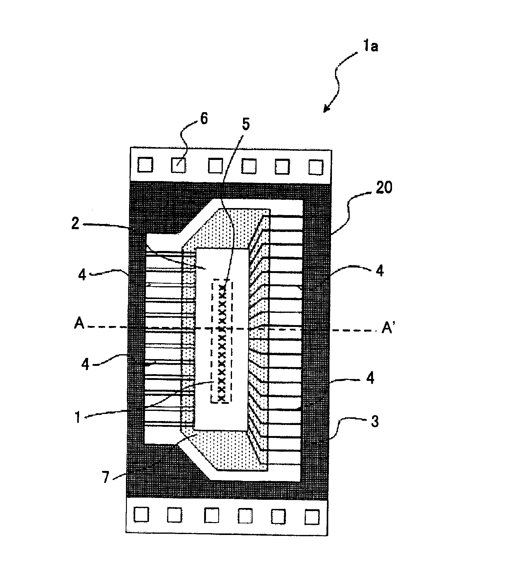
[0037] figure 1 A plan view of a liquid crystal driver package in a semiconductor device according to an embodiment of the present invention is shown.

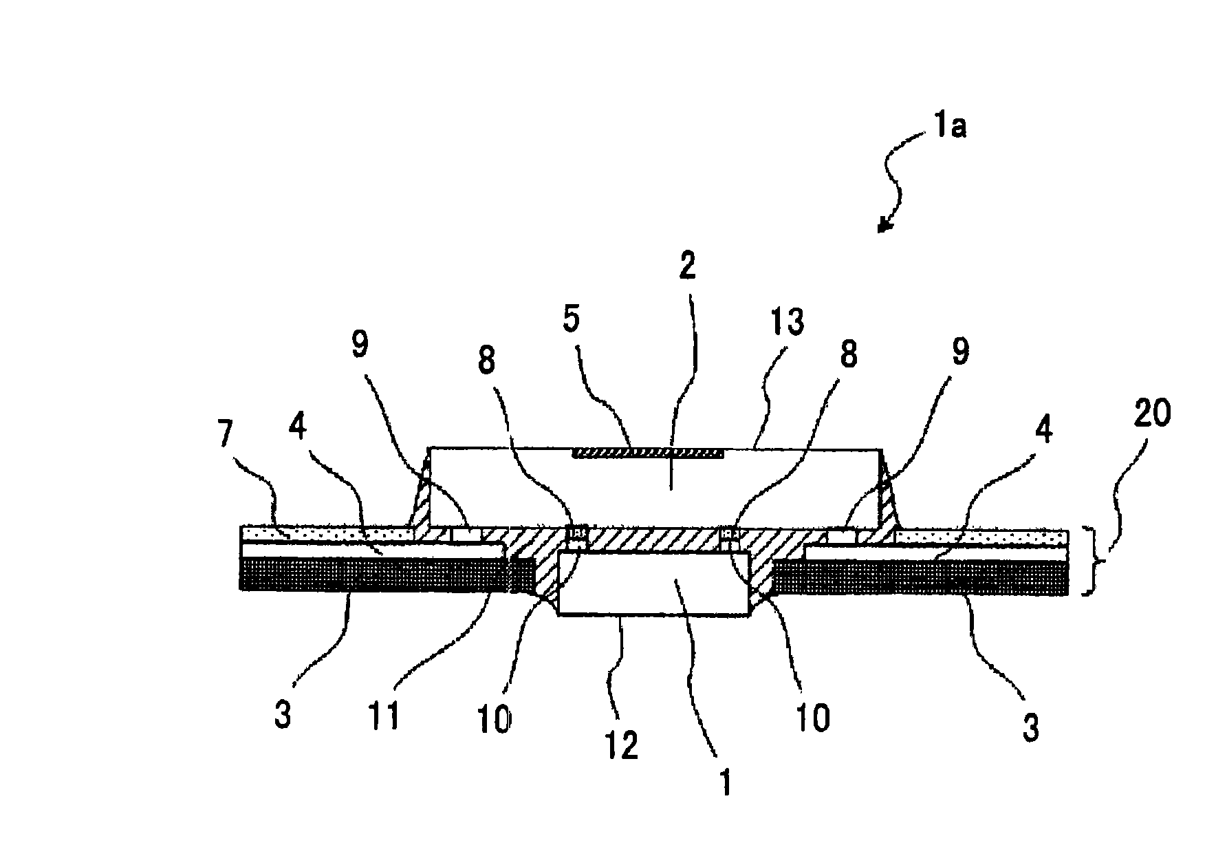
[0038] The liquid crystal driver package 1 a in this embodiment is a COF type package that electrically connects the semiconductor element (liquid crystal driver) 1 and the circuit substrate (carrier tape) 20 through the interposer 2 . exist figure 1 Among them, the liquid crystal driver 1 is disposed on the back of the interposer 2 . Therefore, the liquid crystal driver 1 that cannot be seen actually is shown by a dotted line.

[0039] figure 1 The part shown shows one of the unit packages formed on a long carrier tape, and delivery holes 6 for transporting the long carrier tape are formed at both side edges of the carrier tape. The carrier tape includes: a film substrate 3 mainly composed of polyimide, a wiring pattern 4 made of copper foil formed on one side of the film substrate 3, and an anti-corrosion film for pro...

Embodiment approach 2

[0068] Figure 5 Another example showing the semiconductor device of the present invention is a BGA (Ball Grid Array: Ball Grid Array) type package on which a semiconductor element is mounted. In the figure, the structures having functions equivalent to those of the liquid crystal driver package described above are given the same reference numerals and their descriptions are omitted.

[0069] Semiconductor element (IC chip) 81 is connected with interposer 2 by the mode of flip-chip, and interposer 2 is connected with the wiring pattern 4 that is arranged on the circuit substrate 90, and semiconductor element (IC chip) 81 and interposer 2 are installed on BGA type mounting body 1b.

[0070] The circuit board 90 is made of an insulating substrate 83 such as glass epoxy resin or ceramics, and the wiring pattern 4 formed on the insulating substrate 83 is connected to the soldering bump 85 through a via hole 84, wherein the via hole 84 penetrates the above-mentioned insulating su...


PUM


Abstract

The invention relates to a semiconductor device having an interposer (2) electrically connected to a semiconductor element (1). The interposer (2) has a mark (5) that displays prescribed information relating to the semiconductor element (1).

Description

technical field [0001] The present invention relates to a semiconductor device on which a small semiconductor element is mounted, a display device and electronic equipment including the semiconductor device. Background technique [0002] Liquid crystal display devices are widely used in various devices such as televisions or monitors of personal computers, cellular phones, and the like. In recent years, along with the increase in the amount of information required to be displayed, higher definition and higher performance of liquid crystal display devices have been demanded. Accordingly, liquid crystal drivers, which are semiconductor elements included in liquid crystal display devices, are required to further realize multi-output. In this way, the chip size is reduced by downsizing the driver circuit or fine-pitching bumps provided on the semiconductor element chip, and at the same time realizing multi-output liquid crystal drivers. [0003] The multi-output semiconductor ...

Claims


Application Information

Patent Timeline
Patent Type & Authority Applications(China)
IPC IPC(8): H01L23/00H01L23/12
CPCH01L2924/1532H01L2224/83851H01L24/83H01L21/6836H01L2924/19105H01L2224/2919H01L2221/68327H01L23/544H01L2223/54486H01L24/81H01L2924/01079H01L2224/81203H01L2224/81801H01L2924/09701H01L2224/16G02F1/13452H01L2224/13144H01L2924/15311H01L2223/5448H01L2924/00013H01L2223/54473H01L2223/54433H01L23/4985H01L2924/00011H01L2924/00014H01L2224/13099H01L2224/0401
Inventor 加藤达也久户濑智中川智克
Owner SHARP KK
Why Eureka
Try Eureka