Shift register and grid electrode driving device thereof
A shift register, gate technology, applied in static memory, digital memory information, instruments, etc., can solve problems such as wrong operation, and achieve the effect of low cost
- Summary
- Abstract
- Description
- Claims
- Application Information
AI Technical Summary
Problems solved by technology
Method used
Image
Examples
Embodiment Construction
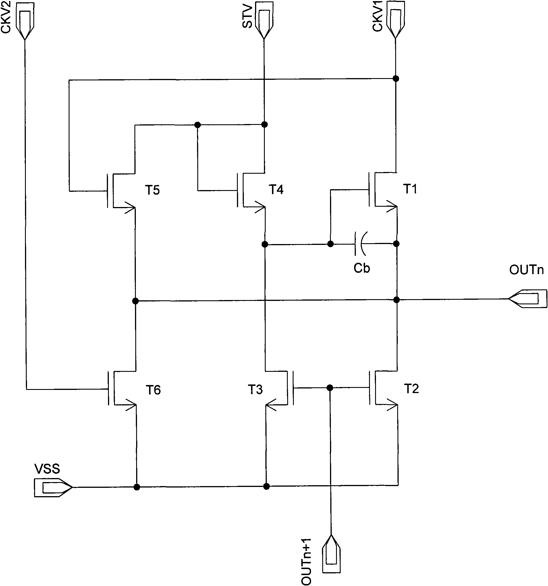
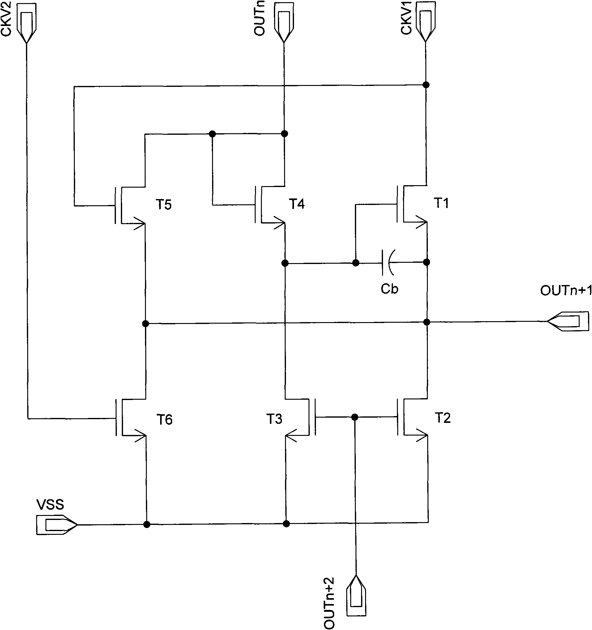
[0022] Figure 1a It is an equivalent circuit diagram of a structure of the shift register of the present invention, Figure 1b It is an equivalent circuit diagram of another structure of the shift register of the present invention. Such as Figure 1a , Figure 1b As shown, the main structure of the shift register of the present invention includes six thin film transistors and corresponding input and output terminals. The six thin film transistors are respectively the first thin film transistor T1, the second thin film transistor T2, the third thin film transistor T3, and the fourth thin film transistor. The transistor T4, the fifth thin film transistor T5 and the sixth thin film transistor T6, the input and output terminals are respectively the output terminal OUTn of the current stage, the output terminal OUTn-1 of the previous stage, the output terminal OUTn+1 of the next stage, and the first clock signal output terminal CKV1, a second clock signal output terminal CKV2, ...
PUM
 Abstract
Description
Claims
Application Information


