Package structure for LED

A technology of light-emitting diodes and packaging structures, applied in the direction of electrical components, electrical solid devices, circuits, etc., to achieve the effects of increasing life cycle, easy implementation, and less heat attenuation

Active Publication Date: 2009-11-11
EPISTAR CORP
View PDF0 Cites 29 Cited by
  • Summary
  • Abstract
  • Description
  • Claims
  • Application Information

AI Technical Summary

Problems solved by technology

Unfortunately, these components have not been able to effectively solve the problem of LED thermal degradation

Method used


Image

  • Package structure for LED
  • Package structure for LED
  • Package structure for LED

Examples


Embodiment Construction

[0040] Preferred embodiments of the present invention are described in detail below. However, those of ordinary skill in the art will recognize the many inventive concepts provided by the present invention, which can be implemented with the widest variation. In addition, the specific embodiments described herein are for illustration only and are not intended to limit the scope of the present invention. scope of protection.

[0041] The preferred embodiment described in the present invention is the packaging structure of LEDs, but the present invention can also be applied to the packaging structures of other different components.

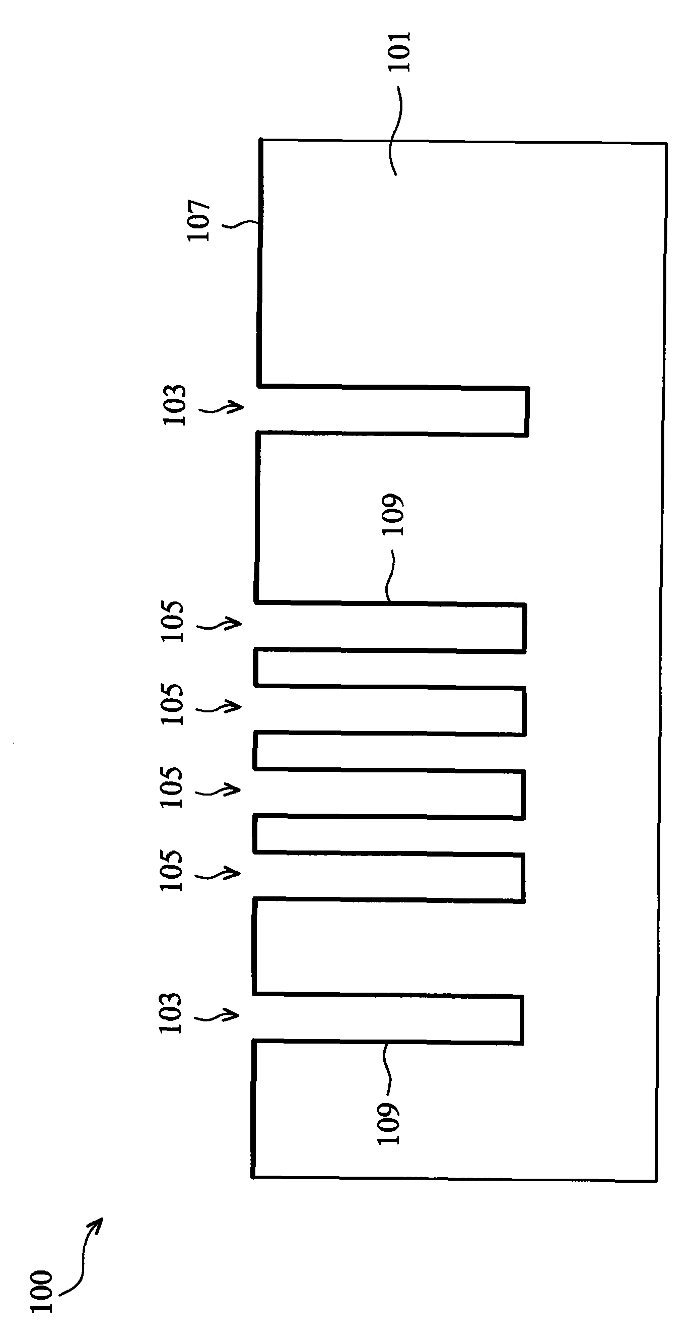
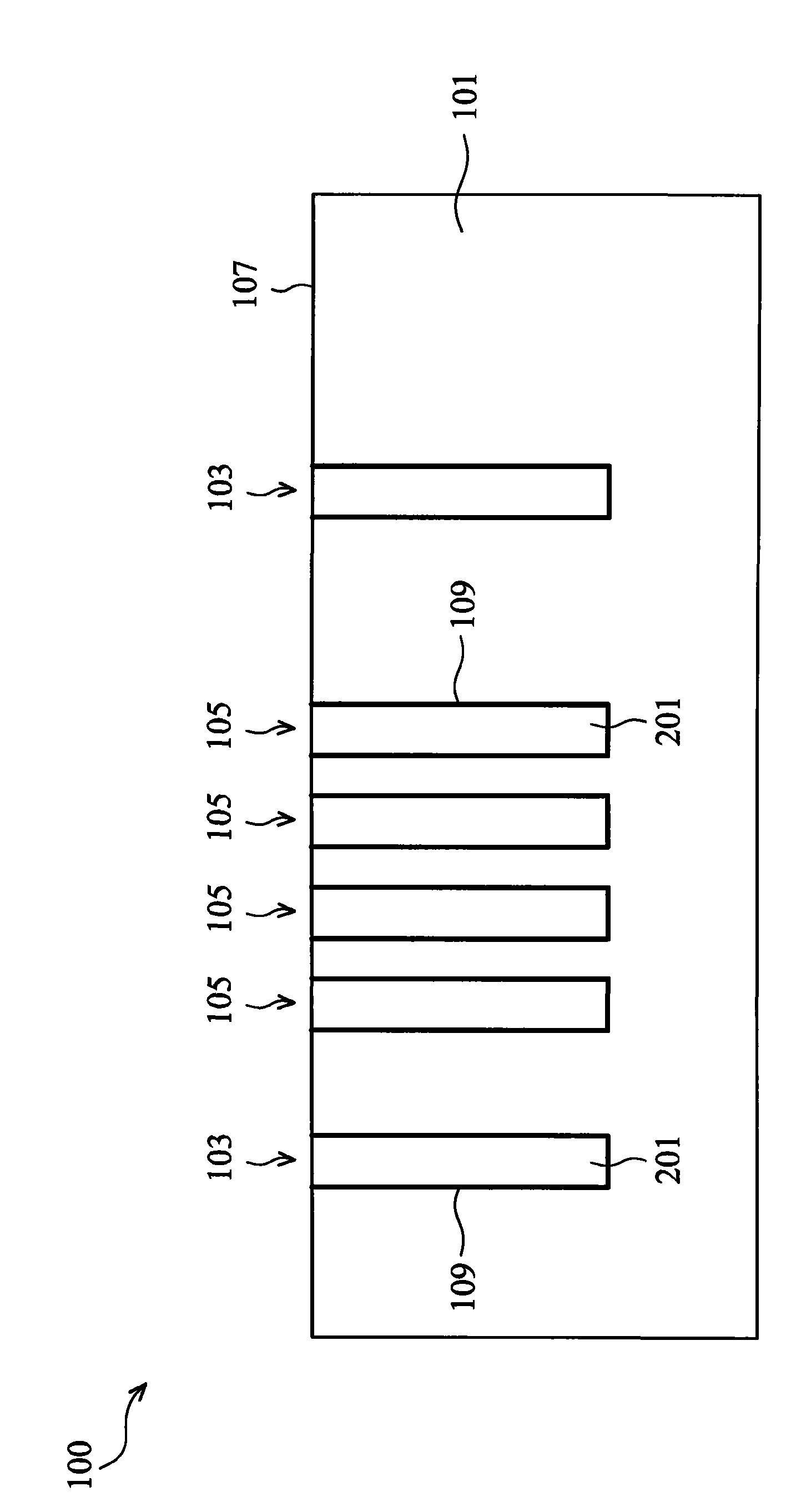
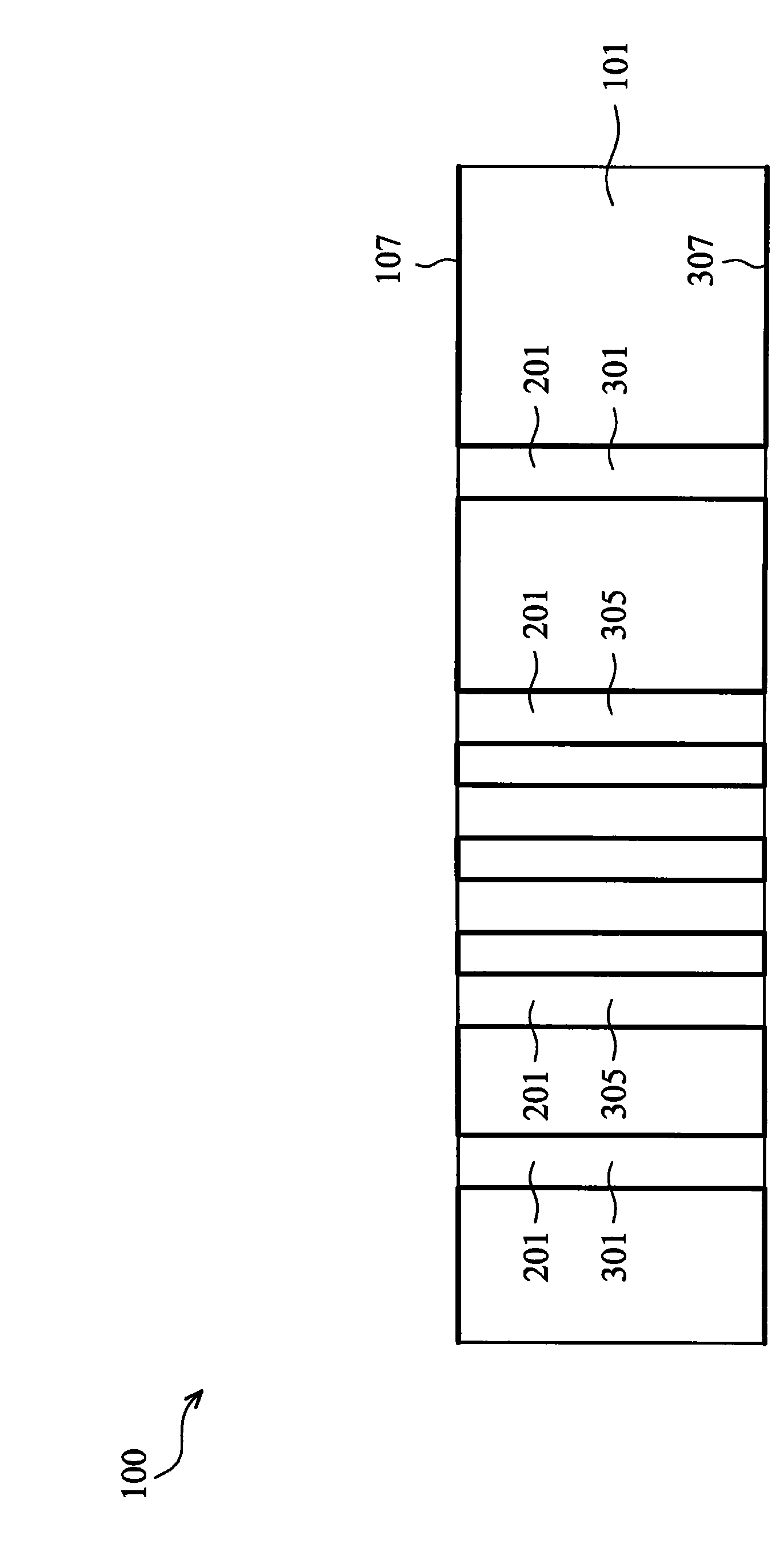
[0042] See figure 1 , which shows a cross-sectional view of a package structure 100 including a substrate 101 and contact openings 103 and thermal openings 105 formed in the substrate 101 . The substrate 101 may include bulk silicon, a doped or undoped substrate, or an active layer of a silicon-on-insulator (SOI) substrate. Generally, a silicon-o...


PUM


Abstract

The invention relates to a package structure for LED and manufacturing method thereof. In a preferred embodiment of the package structure for LED, a plurality of thermal vias are located through the packaging substrate to effectively transfer heat away from the LED, and are preferably formed along with conductive vias that extend through the packaging substrate. The thermal vias are preferably in the shape of circles or rectangular, and may either be solid or else may encircle and enclose a portion of the packaging substrate. Advantage of the preferred embodiment is that heat generated by the LED can be radiated rapidly and effectively by the package structure, less thermal decay is generated, and thereby life circle of the LED in increased.

Description

technical field [0001] The present invention relates to a structure and a manufacturing method of a light emitting diode (LED), and in particular to a structure and a manufacturing method of a packaged LED. Background technique [0002] The demand for LEDs has been increasing over the past few years, especially high brightness and high power LEDs. However, although high-brightness and high-power LEDs can generate a large amount of light, they also generate a large amount of heat, which will cause performance degradation of the LED and shorten the life cycle of the LED. Therefore, heat must be dissipated from the LED as quickly and efficiently as possible. [0003] Recently, in the technical field of LED packaging, a packaging structure using a silicon substrate has been developed. Silicon substrates generally have excellent processability and relatively good thermal conductivity. These silicon substrate packaging structures conduct heat through the silicon substrate itsel...

Claims


Application Information

Patent Timeline
Patent Type & Authority Applications(China)
IPC IPC(8): H01L33/00H01L33/48H01L33/64
CPCH01L33/642H01L33/647H01L33/486H01L33/62H01L2224/16
Inventor 邱文智余振华陈鼎元
Owner EPISTAR CORP
Why Eureka
Try Eureka