
Array substrate and repairing method

A technology of array substrates and common electrode lines, applied in optics, instruments, electrical components, etc., can solve the problem of frequent laser welding times, reduce the times of laser welding and laser cutting, improve repair rhythm, and save man-hours. Effect

Inactive Publication Date: 2009-11-18
SHANGHAI SVA LIQUID CRYSTAL DISPLAY
View PDF0 Cites 4 Cited by
  • Summary
  • Abstract
  • Description
  • Claims
  • Application Information

AI Technical Summary

Problems solved by technology

[0009] The technical problem to be solved by the present invention is to overcome the defects of the prior art that the peripheral common electrode pattern needs to be cut or crossed and the number of times of laser welding is frequent, and to provide a method that can not only keep the peripheral common electrode pattern intact during repair, but also reduce laser welding. Array substrate and repair method for number of passes and cuts

Method used

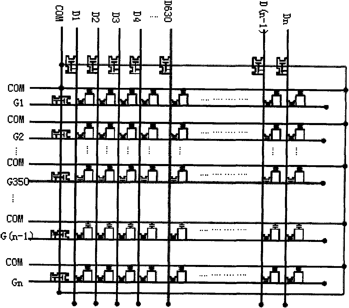
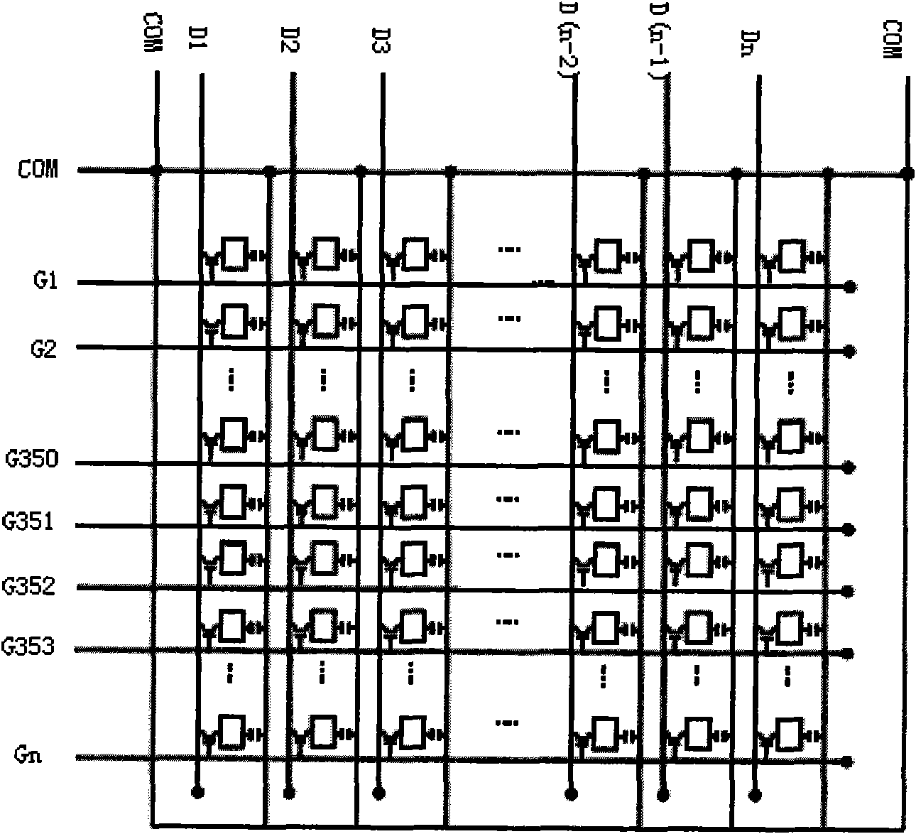
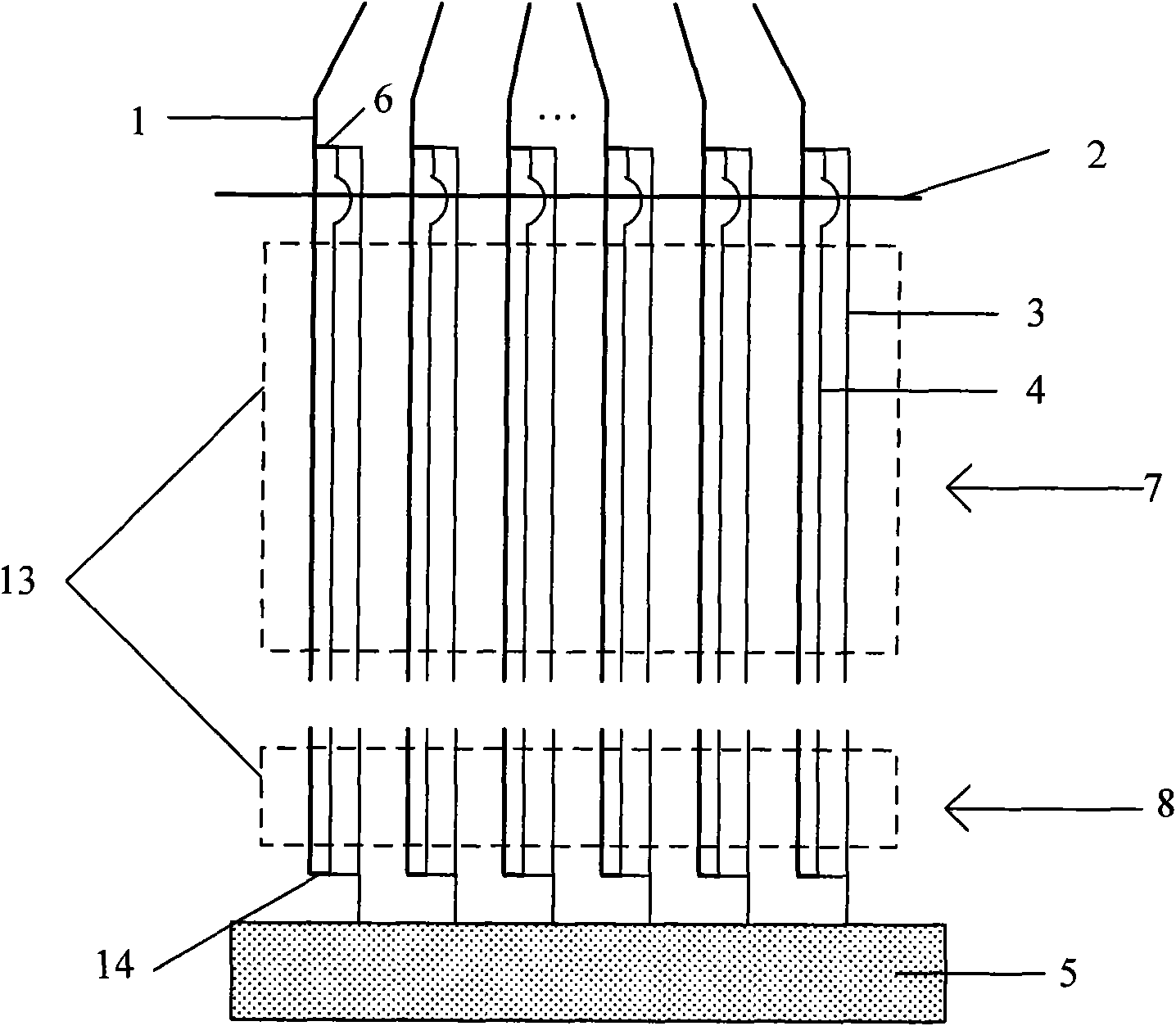

Image

  • Array substrate and repairing method
  • Array substrate and repairing method
  • Array substrate and repairing method

Examples


Embodiment Construction

[0029] The preferred embodiments of the present invention are given below in conjunction with the accompanying drawings to describe the technical solution of the present invention in detail.

[0030] In order to solve the above defects in the prior art, the present invention provides an array substrate, in which each data line corresponds to a first common electrode line, and each first common electrode line is provided with a The second common electrode lines that are connected to each other, and all the common electrode lines and data lines are made of the same layer of metal, and the second common electrode lines are used as repair lines through laser welding and laser cutting, which can repair the corresponding broken lines. The data line is repaired, and at the same time, it can avoid the display failure caused by the existing cutting or passing through the surrounding common electrode pattern.

[0031] Such as image 3 As shown, the data lines 1 , the first common elect...


PUM


Abstract

The invention discloses an array substrate and repairing method. The array substrate comprises a first public electric potential signal wire, a second public electric potential signal wire, a plurality of data wires and a plurality of first public electrode wires, each data wire corresponds to one first public electrode wire, the first public electrode wires are respectively communicated with the first public electric potential signal wire and the second public electric potential signal wire, each first public electrode wire is provided with a second public electrode wire communicated with the first public electrode wire, the second public electrode wires are respectively communicated with a first repairing cross wire and a second repairing cross wire, and the first repairing cross wire and the second repairing cross wire are both crossed with the data wires. The invention can keep a repaired peripheral public electrode pattern complete without lowering the supply capacity of public electrode current, reduces various bad displays caused by the reduction of the supply capacity, can reduce the time of laser welding and laser cutting during the reparation, improves the repairing rhythm in production, and saves the labor hour.

Description

technical field [0001] The invention relates to an array substrate, in particular to an array substrate and a repair method for repairing broken data lines. Background technique [0002] Thin film transistor liquid crystal display (TFT-LCD) has become the most widely used flat-panel display device in the world. It is formed by array substrate, color filter substrate and liquid crystal filled between the two substrates. Determine the orientation of liquid crystal molecules to adjust the polarization direction of light to achieve the purpose of displaying images. [0003] The current array substrate structure mainly includes pixels, scanning lines, data lines, common electrode lines, wiring protection units, crimping electrodes, etc. figure 1 Shown is a brief circuit diagram of an array substrate of a thin film transistor liquid crystal display in the prior art. [0004] Such as figure 1 As shown, the scan lines G1 , G2 . . . Gn and the common electrode lines COM are arrang...

Claims


Application Information

Patent Timeline
Patent Type & Authority Applications(China)
IPC IPC(8): G02F1/13G02F1/1362H01L27/12
Inventor 曹兆铿何剑
Owner SHANGHAI SVA LIQUID CRYSTAL DISPLAY
Learn More