
Power supply wiring configuration in semiconductor integrated circuit

A power wiring and integrated circuit technology, applied in the direction of semiconductor devices, circuits, semiconductor/solid-state device components, etc., can solve problems such as the decline in drive power supply performance, achieve the effect of suppressing the increase of the circuit area and ensuring the connection area

Inactive Publication Date: 2008-03-12
PANASONIC CORP
View PDF1 Cites 2 Cited by
  • Summary
  • Abstract
  • Description
  • Claims
  • Application Information

AI Technical Summary

Problems solved by technology

Moreover, as described in the above Japanese Unexamined Patent Publication, in a power supply structure in which stacked vias are periodically reduced in large quantities, the supply performance of driving power is degraded.

Method used


Image

  • Power supply wiring configuration in semiconductor integrated circuit
  • Power supply wiring configuration in semiconductor integrated circuit
  • Power supply wiring configuration in semiconductor integrated circuit

Examples


no. 1 example

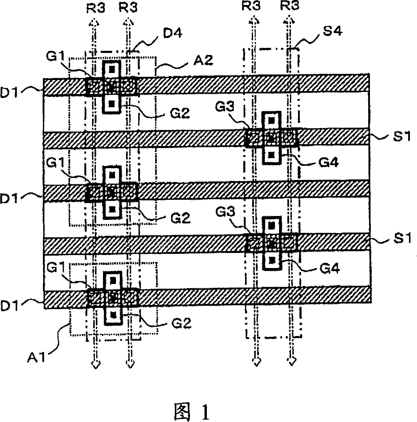
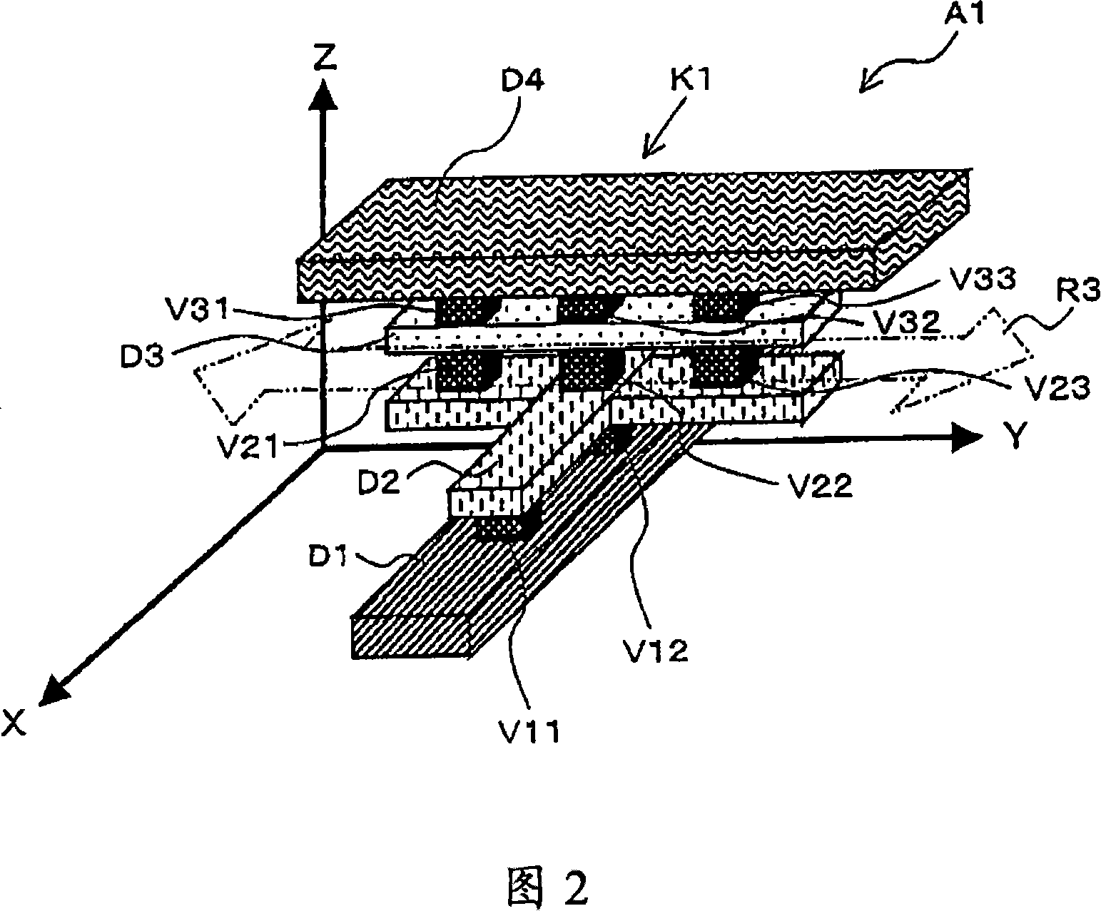
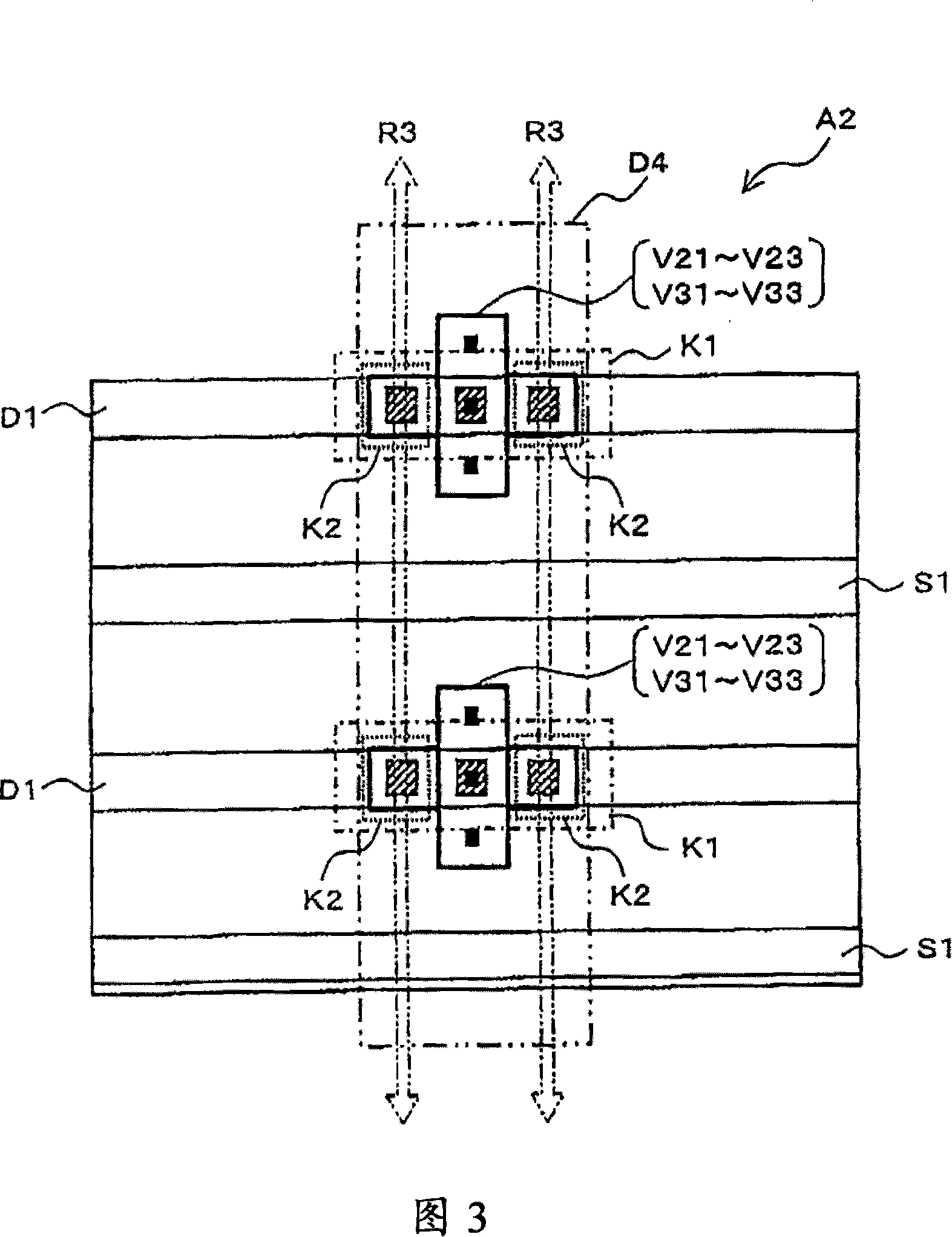
[0033] In FIG. 1 , D1 indicates the VDD power supply wiring (hereinafter, referred to as the lowest VDD power supply wiring) arranged in the lowest wiring layer, and S1 indicates the VSS power supply wiring (hereinafter, referred to as the lowest VSS supply wiring) arranged in the lowest wiring layer. power wiring). The lowest VDD power supply wiring D1 and the lowest VSS power supply wiring S1 extend along the first direction X, and both the power supply wirings D1, S1 are laid alternately along the second direction Y (perpendicular to the first direction) at the same interval. D4 denotes a VDD power supply wiring (hereinafter, referred to as the highest VDD power supply wiring) arranged in the highest wiring layer, and S4 denotes a VSS power supply wiring (hereinafter, referred to as the highest VSS power supply wiring) arranged in the highest wiring layer. The highest VDD power supply wiring D4 and the highest VSS power supply wiring S4 extend along the second direction Y, ...

no. 2 example

[0046] 5 is a power wiring diagram of a semiconductor integrated circuit according to a second embodiment of the present invention. Descriptions of regions having the same structure as those of the first embodiment will be omitted. In FIG. 5, C1 and C2 denote standard cells including transistors. The branch power supply wiring D11 and the branch power supply wiring D12 electrically connected in the same layer and connected to the source of the P-channel transistor at the same potential as the power supply wiring D1 of the lowest layer are laid in the cell C1 along the second direction Y, and Similarly, branch power supply wiring D13 electrically connected within the same layer and connected to the source of the P-channel transistor at the same potential as the lowest power supply wiring D1 is laid in the cell C2 along the second direction Y. The power supply wiring group g1 is a power supply wiring composed of a second intermediate wiring layer and a third intermediate wiring...


PUM


Abstract

A first intermediate power supply wiring is arranged on an upper layer of a lowest power supply wiring arranged along a first direction. A second intermediate power supply wiring is arranged on an upper layer of the first power supply wiring. A third intermediate power supply wiring is arranged on an upper layer of the second intermediate power supply wiring. A highest power supply wiring is arranged along a second direction on an upper layer of the third intermediate power supply wiring. The first intermediate power supply wiring extends from an intersecting region of the highest power supply wiring and the lowest power supply wiring to an outer side of the intersecting region along the first direction. The second intermediate power supply wiring includes a wiring site extending from the intersecting region to the outer side of the intersecting region along the first direction and a wiring site extending from the intersecting region to the outer side of the intersecting region along the second direction. The third intermediate power supply wiring extends from the intersecting region to the outer side of the intersecting region along the second direction. The first intermediate power supply wiring is inter-layer connected to the lowest wiring layer. The second intermediate power supply wiring is inter-layer connected to the first intermediate power supply wiring and the third power supply wiring. The third intermediate power supply wiring is inter-layer connected to the highest wiring layer.

Description

technical field [0001] The present invention relates to a power supply wiring structure in a semiconductor integrated circuit. Background technique [0002] Recently, with the miniaturization of the manufacturing process, the integration density of transistors in LSI has been increased, and the power supply voltage has been reduced at the same time. Therefore, the influence of the voltage drop due to the resistance of the power supply wiring within the LSI chip on the processing speed cannot be ignored. This becomes a cause of increased delay time and malfunctions in logic circuits. Therefore, the design of power wiring is very important. However, since the power supply wiring structure is a structure that occupies most of the wiring area, the increase in the number of power supply wirings and the expansion of the width of the power supply wiring tend to reduce other wiring areas. This results in an increase in integrated circuit area. [0003] In recent power supply wir...

Claims


Application Information

Patent Timeline
Patent Type & Authority Applications(China)
IPC IPC(8): H01L23/528
CPCH01L23/5286H01L2924/0002H01L2924/00
Inventor 清水忠宏
Owner PANASONIC CORP
Learn More