Touch control signal transmitting circuit for touching and controlling display

A touch display and touch signal technology, applied in static indicators, input/output processes of data processing, instruments, etc., can solve problems such as increasing overall weight, difficulty in production, and increased production costs.

Inactive Publication Date: 2009-11-18
CHI HSIN ELECTRONICS CORP
View PDF0 Cites 16 Cited by
  • Summary
  • Abstract
  • Description
  • Claims
  • Application Information

AI Technical Summary

Problems solved by technology

[0003] For the touch panel designed based on the principle of capacitive touch sensing, it is still an individual structure independent of the flat panel display, and its basic structure includes a first electrode layer and a second electrode arranged in an electrically insulating manner layer, the capacitive touch structure must have many contacts in order to provide a more accurate judgment of the touch position, so the first electrode layer and the second electrode layer are composed of a plurality of carefully arranged linear electrodes, and the first The linear electrodes of the electrode layer and the linear electrodes of the second electrode layer are perpendicular to each other, so as to form contacts at the intersections, and each of the linear electrodes is electrically connected to a bonding pad, And each joint pad is electrically connected to the pin (pin) of the touch IC respectively, so that the effect of clearly judging the contact position when the display is in use can be obtained. However, in the case of a larger number of contacts Below, it means that the number of bonding pads and touch IC pins will also increase accordingly, which will inevitably cause difficulties in production, and indirectly increase the overall weight, which will increase the production cost. Therefore, in order not to Under the premise of compromising the function of judging the finger contact position, the production of the touch sensing structure can be simplified, and the design is refined. Based on this, the present invention is finally produced after careful consideration.

Method used


Image

  • Touch control signal transmitting circuit for touching and controlling display
  • Touch control signal transmitting circuit for touching and controlling display
  • Touch control signal transmitting circuit for touching and controlling display

Examples


Embodiment Construction

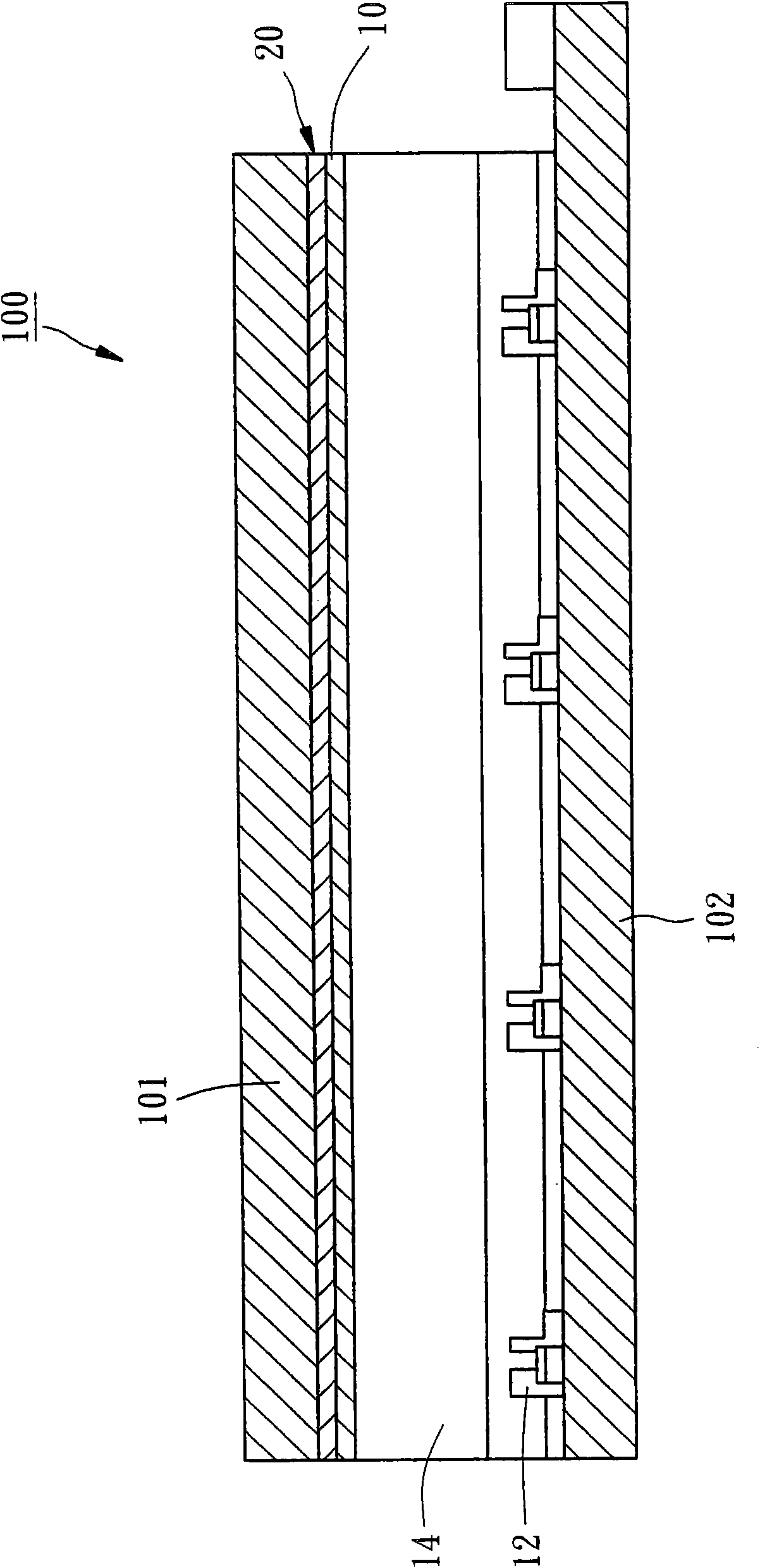
[0034] figure 1 The touch display 100 shown includes an upper substrate 101 and a lower substrate 102, wherein a color filter layer 10 is disposed on the inner surface of the upper substrate 101, and a plurality of thin film transistors 12 arranged in an array are arranged on the surface of the lower substrate 102. Liquid crystal 14 is injected between 101 and lower substrate 102 .

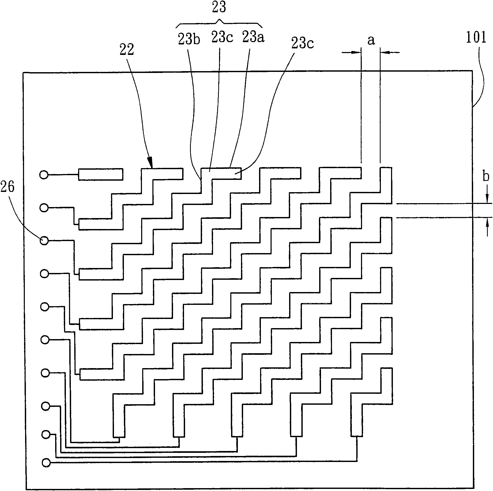
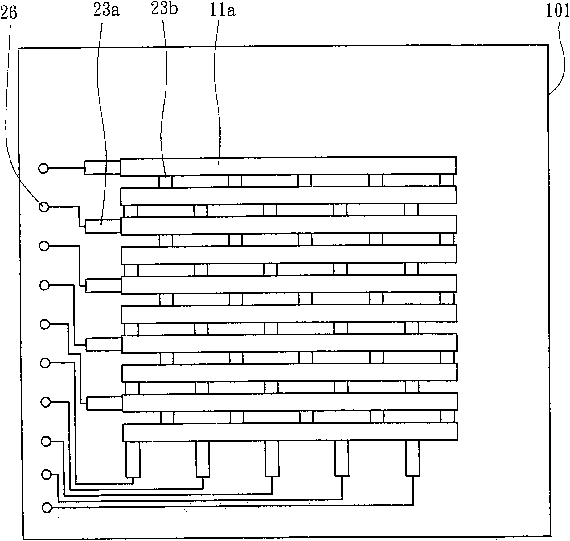
[0035] Please cooperate first Image 6 , the aforementioned color filter layer 10 includes a plurality of red, green, blue filter units 10a, 10b, 10c and a black matrix (Black Matrix, BM) 11, the black matrix 11 is made of insulating black resin material , which has a plurality of horizontal first shading elements 11a and a plurality of vertical second shading elements 11b, the first shading elements 11a and the second shading elements 11b alternately surround and form a plurality of isolation regions 11c for the red , green, and blue filter units 10a, 10b, and 10c are configured, and the touch ...


PUM


Abstract

The invention relates to a touch control signal transmitting circuit for touching and controlling a display, which is arranged on the inner surface of an upper base plate of a display. The transmitting circuit comprises a first patterned electrode layer and a second patterned electrode layer which are electrically insulated and are overlapped up and down. The first patterned electrode layer and the second patterned electrode layer respectively comprise a plurality of stepped electrodes; and moreover, the stepped electrodes of the first patterned electrode layer and the stepped electrodes of the second patterned electrode layer are alternately arranged, and each upper and lower opposite position forms an induction contact. Therefore, the whole touch control induction zone can be covered by only arranging a small amount of stepped electrodes, and thus, the using amount of joint liners and touch control IC pins can be reduced. In addition, because a plurality of induction contacts are still distributed densely in the touch control induction zone, the functions of quick detection and quick judgment can be maintained.

Description

technical field [0001] The present invention relates to a control structure of a liquid crystal display, and more specifically refers to a touch signal transmission circuit of a touch-sensitive liquid crystal display. Background technique [0002] A general touch display is assembled by stacking a touch panel and a flat-panel display up and down, but this type of display structure is prone to increase the overall thickness and increase the weight, which is in line with the current design concept towards thinner and shorter Therefore, while actively seeking to optimize the display effect, the industry is also committed to the development and design of reducing the thickness and weight of the display. [0003] For the touch panel designed based on the principle of capacitive touch sensing, it is still an individual structure independent of the flat panel display, and its basic structure includes a first electrode layer and a second electrode arranged in an electrically insulat...

Claims


Application Information

Patent Timeline
Patent Type & Authority Applications(China)
IPC IPC(8): G02F1/133G02F1/1343G06F3/041G06F3/044
Inventor 赖辉龙
Owner CHI HSIN ELECTRONICS CORP
Why Eureka
Try Eureka