Display panel and signal transmission method thereof

A display panel and signal transmission technology, which is applied in static indicators, nonlinear optics, instruments, etc., can solve the problems of power receiving pad P being burned, unable to display images and screens, and unable to open the display unit 103 smoothly, etc.

Active Publication Date: 2012-11-14
HANNSTAR DISPLAY CORPORATION
View PDF3 Cites 0 Cited by
  • Summary
  • Abstract
  • Description
  • Claims
  • Application Information

AI Technical Summary

Problems solved by technology

Also because of this, when the liquid crystal display is turned on and off, an excessive inrush current (inrush current) is likely to flow into the gate drive voltage V GH The power receiving pad P GH , causing the power receiving pad P GH burnt
In this way, not only will the gate driver chips 101a˜101n fail to turn on the pixels of each scanning line in the display unit 103 smoothly, but also the display unit 103 will not be able to display images for users to watch.

Method used


Image

  • Display panel and signal transmission method thereof
  • Display panel and signal transmission method thereof
  • Display panel and signal transmission method thereof

Examples


Embodiment Construction

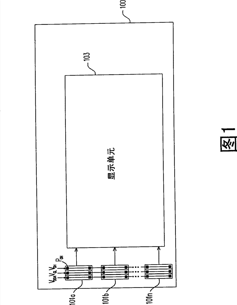
[0043]The main purpose of the present invention is to effectively suppress the possibility of burning the power receiving pads of any gate drive chip directly arranged on the glass substrate of the liquid crystal display panel at the moment of switching on and off the liquid crystal display, and the following The content will provide a detailed description of the technical features and desired effects of the present invention, so as to provide reference for those skilled in the relevant fields of the present invention.

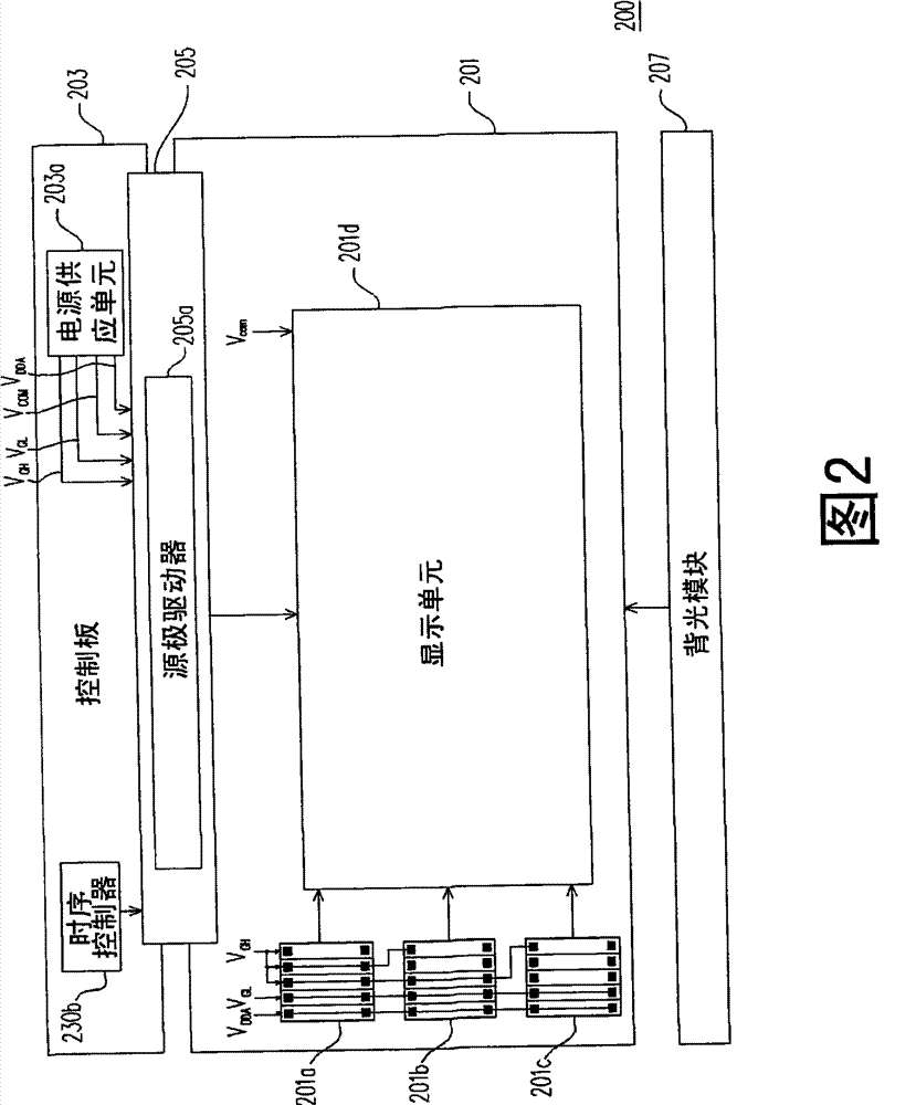
[0044] figure 2 A schematic diagram of the system architecture of the liquid crystal display 200 according to an embodiment of the present invention is shown. refer to figure 2 , a liquid crystal display (LCD) 200 includes a liquid crystal display panel (LCD panel) 201, a control board (control board) 203, a flexible printed circuit board (flexible printed circuit board, FPC) 205, and is used to provide a backlight for the liquid crystal display panel 201 ...


PUM


Abstract

The invention discloses a display panel and a signal transmission method thereof. The display panel provided by the invention comprises a substrate and at least a first driving chip and a second driving chip. The first and second driving chips are directly arranged on one side of the substrate; the first driving chip is at least provided with a first power supply receiving solder pad, first and second auxiliary solder pads and a first auxiliary wire; and the second driving chip is at least provided with a second power supply receiving solder pad. The first power supply receiving solder pad and the first auxiliary solder pad are used for receiving system voltages respectively and the first auxiliary solder pad is also connected with the second auxiliary solder pad through the first auxiliary wire to transmit the system voltage to the second power supply receiving solder pad from the second auxiliary solder pad.

Description

technical field [0001] The present invention relates to a plane display technology, and in particular to a power wiring and a signal transmission method between a plurality of gate drive chips directly arranged on a glass substrate of a liquid crystal display panel. Background technique [0002] With the evolution of optoelectronics and semiconductor technology, it has also led to the vigorous development of flat-panel displays. Among many flat-panel displays, liquid crystal displays (LCD) have high space utilization efficiency, low power consumption, no radiation and low Superior features such as electromagnetic interference have immediately become the mainstream of the market. [0003] In recent years, in order to effectively control the production cost of liquid crystal displays, some panel manufacturers have adopted a chip-on-glass (COG) bonding process to directly connect multiple gate drive chips. It is arranged on one side of the glass substrate of the panel, thereby...

Claims


Application Information

Patent Timeline
Patent Type & Authority Patents(China)
IPC IPC(8): G02F1/13G09G3/36
Inventor 曾祥云王杰会林文奇
Owner HANNSTAR DISPLAY CORPORATION
Why Eureka
Try Eureka