


Quick Research
Generate reliable direction feasibility study reports for your R&D in just a few steps.

Technical Q&A
Discover and master advanced knowledge NOW. Basics, ideas, possibilities, all at once.

Find Solutions
As an expert in R&D theories, this can generate solutions to your technical problems instantly.

Evaluate Feasibility
Analyze your overall solution with one click, know your potential R&D risks in advance.

Monitor Landscape
Get weekly tech updates, stay abreast of the latest tech innovations and key insights.
Method for manufacturing semiconductor device by using dual damascene process and method for manufacturing article having communicating hole
A dual damascene process, semiconductor technology, applied in semiconductor/solid-state device manufacturing, electrical components, circuits, etc.
- Summary
- Abstract
- Description
- Claims
- Application Information
AI Technical Summary
Problems solved by technology
Method used
Image

Examples
no. 1 example
[0035] will refer to Figure 1A and 1B A first embodiment according to an aspect of the present invention will be described.
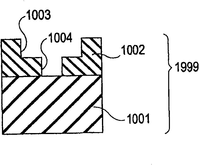
[0036] A member 1999 ( Figure 1A ).
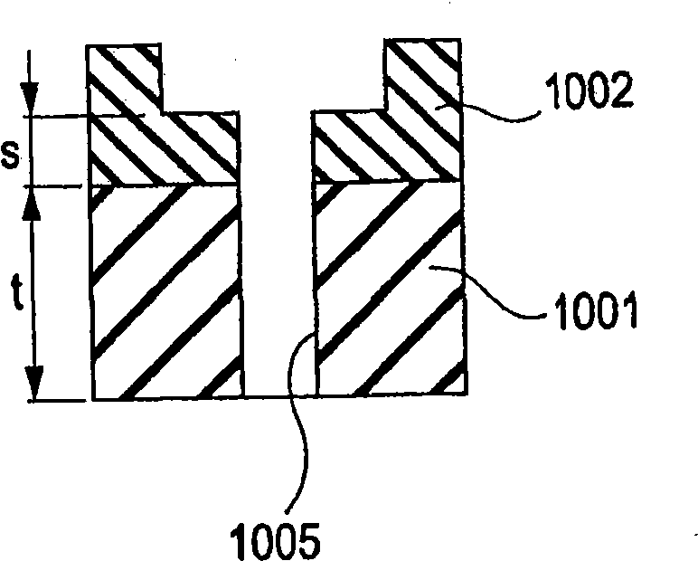
[0037] The above-mentioned second insulating film 1002 is produced by embossing a pattern (not shown in the drawings) on the layer after providing a layer on the above-mentioned first insulating film 1001, and the pattern corresponds to the wiring groove 1003 and the first insulating film 1002. A through hole 1004 .
[0038] For example, when contacted with the above-mentioned mold, the material constituting the layer is solidified, thereby producing the second insulating film.
[0039] In the present invention, the layer also includes the case where the material for forming the second insulating film is in the form of a layer on the first insulating film macroscopically, but is in the form of dots microscopically.
[0040] Furthermore, in the present invention, the layer includes the case where the material for ...
no. 2 example
[0103] Second Example: Planarization
[0104] A second embodiment according to another aspect of the present invention is a method of manufacturing a semiconductor device by using the above-mentioned dual damascene process. However, it is characterized by including the step of preparing a member having a first insulating film on a substrate, wherein the first insulating film has been subjected to planarization.
[0105] will refer to Figures 6A to 6E This embodiment will be described.
[0106] exist Figure 6A , reference numeral 1800 denotes an uneven substrate.
[0107] Here, the substrate includes a substrate composed of a multilayer film. The above-mentioned multilayer film includes a conductive layer formed of Cu or the like or an insulating layer formed of SiC or the like.
[0108] A first insulating film 1801 is provided on a substrate 1800, and the first insulating film 1801 has been subjected to a planarization process in order to reduce unevenness.
[0109] Th...
no. 3 example
[0129] The third embodiment: optical printing
[0130] The method for manufacturing the semiconductor device according to the third embodiment of the present invention is performed as follows.
[0131] A member having a first insulating film is prepared on a substrate.
[0132] Furthermore, a model having patterns corresponding to the wiring trenches and the first via holes is prepared.
[0133] An ultraviolet curable resin layer is inserted between the mold and the first insulating film, and the resin layer is irradiated with ultraviolet rays to be cured.
[0134] After curing the resin, the above-mentioned mold and resin are separated from each other. If necessary, the above cured resin is subjected to anisotropic etching (so-called etch-back step).
[0135] In this way, the second insulating film having the aforementioned wiring trench and the aforementioned first via hole can be produced.
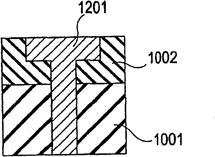
[0136] The above-mentioned first insulating film is selectively etched by using...
PUM
 Abstract
Description
Claims
Application Information
 - R&D Engineer
- R&D Manager
- IP Professional
- Industry Leading Data Capabilities
- Powerful AI technology
- Patent DNA Extraction
Browse by: Latest US Patents, China's latest patents, Technical Efficacy Thesaurus, Application Domain, Technology Topic, Popular Technical Reports.
© 2024 PatSnap. All rights reserved.Legal|Privacy policy|Modern Slavery Act Transparency Statement|Sitemap|About US| Contact US: help@patsnap.com