Flash memory control device with sequential write and control method

A flash memory control and flash memory technology, which is applied in the direction of memory address/allocation/relocation, etc., can solve the problems of the write efficiency reduction of non-AND type flash memory and the reduction of write efficiency of non-AND type flash memory, etc.

Inactive Publication Date: 2010-03-17
GENESYS LOGIC INC
View PDF0 Cites 2 Cited by
  • Summary
  • Abstract
  • Description
  • Claims
  • Application Information

AI Technical Summary

Problems solved by technology

Writing to non-AND flash memory is less efficient due to having to perform multiple write procedures
Especially when a large amount of data is to be transferred to the non-AND flash memory, and the write commands and addresses related to the data are sent to the non-AND flash memory one by one through the flash controller, the write efficiency of the non-AND flash memory is serious. reduce

Method used


Image

  • Flash memory control device with sequential write and control method
  • Flash memory control device with sequential write and control method
  • Flash memory control device with sequential write and control method

Examples


Embodiment Construction

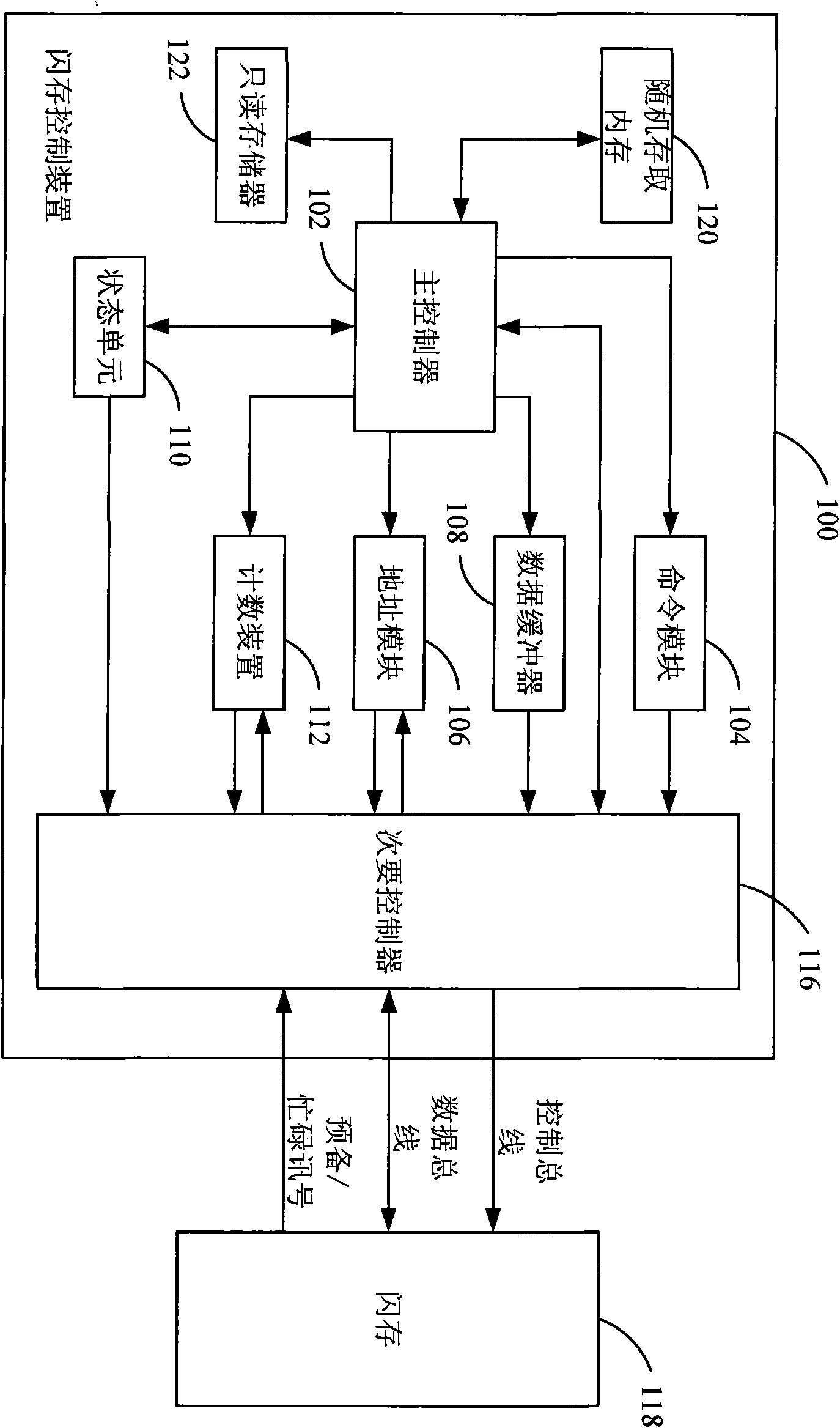
[0013] figure 1 It is a block diagram of a flash memory control device 100 with sequential writing according to an embodiment of the present invention. The flash memory control device 100 mainly includes a main controller 102, a command module 104, an address module 106, a data buffer 108, a status unit 110, a counting device 112, a memory unit 114, and a secondary controller 116.

[0014] The flash memory control device 100 is coupled to the flash memory 118 via a number of control buses, data buses, and ready / busy control signal lines. In one embodiment, the main controller 102 is, for example, an 8051 type chip or various types of digital signal processors (digital signal processors, DSP), and the command module 104 is, for example, a register for storing commands. The address module 106 is, for example, a register for storing addresses related to the data and commands. The secondary controller 116 is, for example, a flash controller to allow the main controller 102 to control...


PUM


Abstract

The invention discloses a flash memory control device with sequential write and a control method thereof. The flash memory control device comprises a main controller, a command module, an address module, a data buffer, a state unit and a counting device, wherein the main controller generates a preset value; the command module stores a write command in a period of executing a write procedure; the address module stores a current address and carries out addressing of a current page; the data buffer stores data; the state unit decides that a flash memory is in a standby mode or a busy mode; and when the command module correctly writes the data to the current page, the address module generates at least one downstream adjacent address, and the command module orderly and continuously write the data to at least one downstream adjacent page so as to completely and continuously write the data to all the pages in the period of executing the write procedure.

Description

【Technical Field】 [0001] The present invention relates to a memory device and a method thereof, and more particularly to a flash memory control device with sequential writing and a control method thereof. 【Background technique】 [0002] The Not AND (NAND) flash memory is composed of a number of blocks, and each block includes a number of data pages. The size of the small block is 512 bytes (bytes), and the size of the large block is 2048 bytes (bytes). The current NAND flash memory (NAND flash memory) uses the block as the minimum write unit. Although the real smallest unit of the NAND flash memory is the data page, it is limited by the fact that the NAND flash memory needs to write data. The technical architecture of the block needs to be erased first, so that the actual minimum write unit of the non-AND type flash memory is a block. [0003] Generally speaking, when the conventional non-AND type flash memory does not support sequential writes, the non-AND type flash memory flas...

Claims


Application Information

Patent Timeline
Patent Type & Authority Applications(China)
IPC IPC(8): G06F12/02
Inventor 林璟鸿黄玮淦李浩纬
Owner GENESYS LOGIC INC
Why Eureka
Try Eureka