Tft panel substrate inspecting device

A substrate inspection and panel technology, applied in the field of detector frames, to achieve the effects of reducing warpage, reducing part prices, and reducing weight

Inactive Publication Date: 2012-02-29
SHIMADZU SEISAKUSHO CO LTD
View PDF3 Cites 0 Cited by
  • Summary
  • Abstract
  • Description
  • Claims
  • Application Information

AI Technical Summary

Problems solved by technology

[0014]It can be predicted that with the advancement of the size of TFT panel substrates and mother glass substrates, it is difficult to cope with the rigidity of the detector frame

Method used


Image

  • Tft panel substrate inspecting device
  • Tft panel substrate inspecting device
  • Tft panel substrate inspecting device

Examples


Embodiment Construction

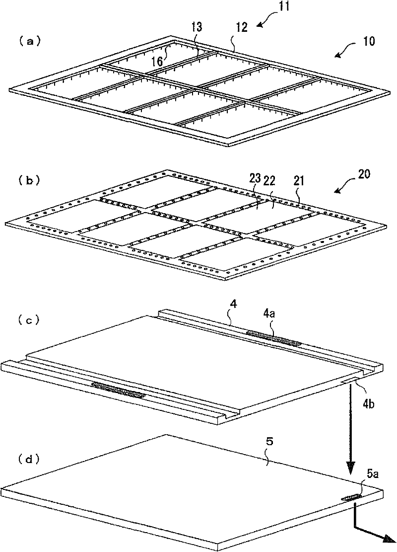
[0073] Below, while referring to the attached Figure 1 Embodiments of the present invention will be described in detail.

[0074] figure 1 (a)-(d) is a figure for demonstrating the structure of the probe unit used for the TFT panel board|substrate inspection apparatus of this invention. Hereinafter, the case where a liquid crystal panel is used as a TFT panel substrate will be described as an example.

[0075] The liquid crystal panel 20 is an inspection object inspected by the TFT panel substrate inspection device 1 , and a TFT array 23 is formed on the TFT panel substrate 21 . The layout of the TFT array 23 formed on the TFT panel substrate 21 is variously set according to the size and specifications of the liquid crystal panel, for example. Thin film transistors are formed in a matrix in the TFT array 23 on the TFT panel substrate 21 , and signal electrode terminals (for example, scanning signal electrode terminals and video signal electrode terminals) for driving the ...


PUM


Abstract

A TFT panel substrate inspecting device includes an electron beam generating source for performing irradiation with an electron beam, a second electron detector for detecting a second electron generated from a pixel by the irradiation with the electron beam, and a voltage application unit composed of a plurality of probe pins for applying a reference voltage to an electrode on a plurality of TFT panel substrates by coming into contact with the electrode. The voltage application unit includes a prober frame surrounding the outer periphery of the TFT panel substrate. The prober frame includes at least one inner frame surrounding the TFT panel substrate and a rim-like outer frame surrounding the inner frame inwardly. The flexure of the inner frame generated by the weight of the inner frame and the reactive force of the probe pin is reduced and the surface rigidity is increased by attaching the inner frame to the inner periphery wall of the outer frame, applying a pulling load thereto. Consequently, contact pressure between each probe pin and the electrode of the TFT panel substrate is uniformized.

Description

technical field [0001] The present invention relates to a TFT panel substrate inspection device, the TFT panel substrate inspection device includes a liquid crystal display (liquid crystal display) or an organic electroluminescence (electroluminescence, EL) display used in a flat panel display (flat panel display) The TFT panel substrate of the thin-film transistor (thin-film transistor, TFT) array (array) is inspected; the present invention particularly relates to a probe frame (prober frame) for supplying inspection driving signals to the TFT panel substrate. Background technique [0002] In the manufacturing process of a panel of a flat panel display, a plurality of panels including a pattern of a TFT array are usually formed on a mother glass substrate, and each panel is cut out from the mother glass substrate. In the manufacture and inspection of such flat panel displays, it is necessary to evaluate the TFT panel substrate in the state of the mother glass substrate bef...

Claims


Application Information

Patent Timeline
Patent Type & Authority Patents(China)
IPC IPC(8): G01R31/00
CPCG09G3/006G01R31/305
Inventor 芝吹直伸铃木正康
Owner SHIMADZU SEISAKUSHO CO LTD
Why Eureka
Try Eureka