
Polydomain array method of multiple light-emitting diode chips under single lens

A light-emitting diode and single-lens technology, applied in the field of multi-domain arrangement, can solve problems such as inconvenience and poor light mixing effect, and achieve the effect of uniform light mixing and reducing the overall volume

Inactive Publication Date: 2010-03-31
HELIO OPTOELECTRONICS
View PDF0 Cites 0 Cited by
  • Summary
  • Abstract
  • Description
  • Claims
  • Application Information

AI Technical Summary

Problems solved by technology

[0006] like Figure 4A As shown, due to the relative arrangement position of the LED chips of different colors in space, and the influence of the mirror axis 11 of the hemispherical lens 10 and the direction of the light-emitting axis 12 of each LED chip, the light is emitted under the hemispherical lens 10. The light patterns of the red light-emitting diode chip, green light-emitting diode chip and blue light-emitting diode chip are as follows Figure 4B , Figure 4C and Figure 4D As shown, it is an asymmetrical light type, so polarized light is generated, resulting in poor light mixing effect at the edge of the hemispherical lens 10
[0007] It can be seen that the method and use of multiple light-emitting diode chips under the above-mentioned existing single lens obviously still have inconvenience and defects, and it is urgent to be further improved.
In order to solve the above-mentioned existing problems, relevant manufacturers have tried their best to find a solution, but no suitable design has been developed for a long time. This is obviously a problem that relevant manufacturers are eager to solve.

Method used


Image

  • Polydomain array method of multiple light-emitting diode chips under single lens
  • Polydomain array method of multiple light-emitting diode chips under single lens
  • Polydomain array method of multiple light-emitting diode chips under single lens

Examples


no. 1 example

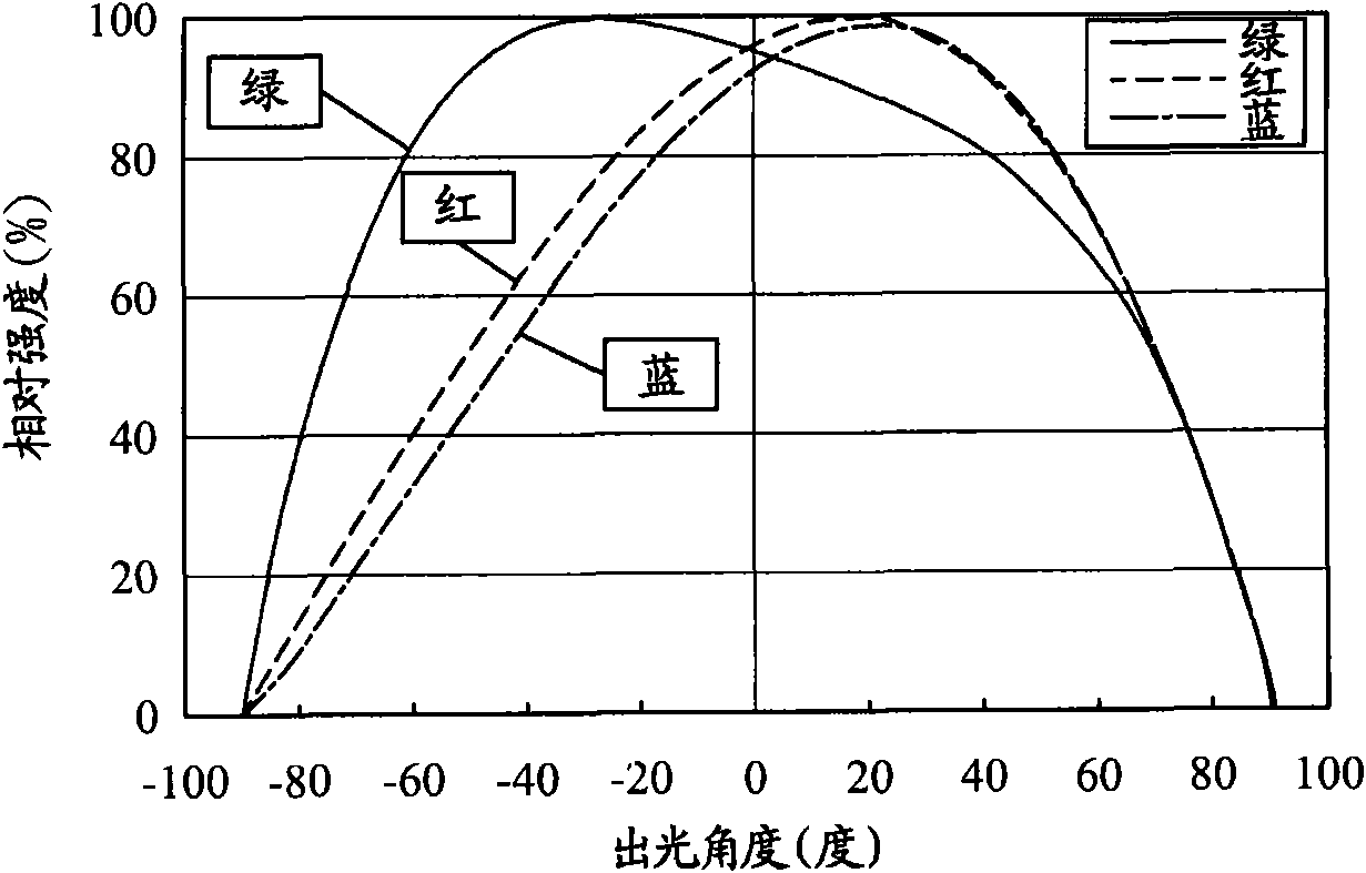
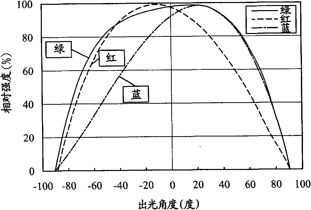
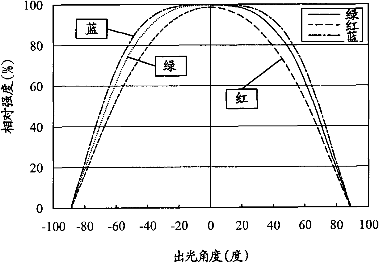
[0091] see Figure 5 , Image 6 , Figure 7 , Figure 8A , Figure 8B , 8C , Figure 8D , Figure 9 as shown, Figure 5 It is a flow embodiment of the multi-domain arrangement method S10 of multiple light-emitting diode chips under a single lens of the present invention Figure 1 . Image 6 It is a three-dimensional decomposition embodiment of a multi-domain arrangement method S10 of multiple light-emitting diode chips under a single lens of the present invention Figure 1 . Figure 7 It is an embodiment of the multi-domain arrangement method S10 of multiple light-emitting diode chips under a single lens of the present invention Figure 1 . Figure 8A yes Figure 7 A three-dimensional embodiment diagram. Figure 8B yes Figure 7 The light pattern diagram of the red chip in the figure. Figure 8C is along Figure 8A The light pattern diagram of the red chip in the direction of the arrow in A. Figure 8D is along Figure 8A The light pattern diagram of the red ch...

no. 2 example

[0100] see Figure 10 , Figure 11 , Figure 12 , Figure 13 , Figure 14 as shown, Figure 10 It is a flow embodiment of the multi-domain arrangement method S10' of multiple light-emitting diode chips under a single lens of the present invention Figure II . Figure 11 It is a multi-domain arrangement method S10' three-dimensional decomposition embodiment of multiple light-emitting diode chips under a single lens of the present invention Figure II . Figure 12 It is an embodiment of the multi-domain arrangement method S10' of multiple light-emitting diode chips under a single lens of the present invention Figure three . Figure 13 Figure 4 is an embodiment of a multi-domain arrangement method S10' for multiple light emitting diode chips under a single lens of the present invention. Figure 14 It is an embodiment of the multi-domain arrangement method S10' of multiple light-emitting diode chips under a single lens of the present invention Figure five .

[0101] S...

no. 3 example

[0112] see Figure 15 , Figure 16 , Figure 17 as shown, Figure 15 It is a flow embodiment of the multi-domain arrangement method S10" of multiple light-emitting diode chips under a single lens of the present invention Figure three . Figure 16 It is a multi-domain arrangement method S10" stereoscopic decomposition embodiment of multiple light-emitting diode chips under a single lens of the present invention Figure three . Figure 17 It is an embodiment of the multi-domain arrangement method S10" of multiple LED chips under a single lens of the present invention Figure six .

[0113] Such as Figure 15 As shown, the present embodiment is a multi-domain arrangement method S10" for multiple light-emitting diode chips under a single lens, which includes the following steps: setting a fourth color chip S17; setting a fourth concentric circle S18; and arranging multiple a second color chip and a plurality of third color chips S19.

[0114] Set a fourth color chip S17:...


PUM


Abstract

The invention relates to a polydomain array method of multiple light-emitting diode chips under a single lens, comprising the following steps: setting a first concentric circle; and arraying at leastone first chip, one second chip and one third chip. The first concentric circle is formed on the bottom side of a semispherical lens by taking a lens axis of the semispherical lens as the center of circle, and chips with various colors are sequentially arrayed on the first concentric circle in an equal interval mode, thus the chips with various colors can be in a symmetrical light shape under thesemispherical lens and a light field with even mixed light can be further obtained. In addition, the polydomain array method of the multiple light-emitting diode chips under the single lens can ensurethat the multiple light-emitting diode chips form the densest array, thus the overall volume can be reduced.

Description

technical field [0001] The invention relates to a multi-domain arrangement method of multiple light-emitting diode chips under a single lens, in particular to a multi-domain arrangement method applied to color mixing of multiple light-emitting diode chips under a single lens. Background technique [0002] figure 1 It is one of the outgoing light patterns of the prior known hemispherical lens 10 . figure 2 It is the second light emitting pattern of the conventional hemispherical lens 10 . image 3 It is the outgoing light pattern diagram of the existing conventional planar lens. [0003] Such as figure 1 and figure 2 As shown, they are respectively the light-emitting mode 1 and mode 2 of the conventional hemispherical lens 10 . It is through two different viewing angles to measure the light pattern of the light emitting diode chips of each color passing through the hemispherical lens 10. From the measurement results, it can be found that due to the mirror axis 11 of th...

Claims


Application Information

Patent Timeline
IPC IPC(8): H01L25/00H01L25/075
Inventor 王志明何宜霖温士逸曾柏铭林钧闵
Owner HELIO OPTOELECTRONICS
Features
  • Generate Ideas
  • Intellectual Property
  • Life Sciences
  • Materials
  • Tech Scout
  • Unparalleled Data Quality
  • Higher Quality Content
  • 60% Fewer Hallucinations
Learn More