Lateral DMOS transistor and method of fabricating thereof
A technology of transistors and body regions, which is applied in semiconductor/solid-state device manufacturing, semiconductor devices, electrical components, etc., and can solve problems such as the limitation of drain-source impedance
- Summary
- Abstract
- Description
- Claims
- Application Information
AI Technical Summary
Problems solved by technology
Method used
Image

Examples
Embodiment Construction
[0021] Reference will now be made in detail to specific embodiments of the invention, examples of which are illustrated in the accompanying drawings. Wherever possible, the same reference numbers will be used throughout the drawings to refer to the same or like parts.
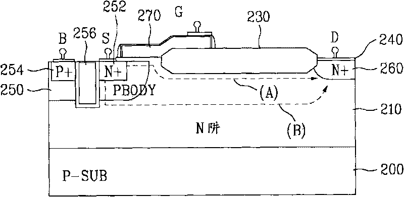
[0022] figure 2 A cross-sectional view showing an LDMOS transistor according to a preferred embodiment of the present invention is shown. refer to figure 2 , the LDMOS transistor includes: N well 210, formed on the P-type semiconductor substrate 200; LOCOS 230, formed on the surface of the N well 210; drain region 260, formed in the N well 210, on one side of the LOCOS 230; and doped N + Type impurity source region 252, doped with P + Type impurity source contact region 254; and a second gate electrode 256 having a trench shape, formed in the P-type body region 250, which is separated from the drain region 260 by a certain distance, in the LOCOS 230 on the other side of the .
[0023] Source region 252 ...
PUM
 Abstract
Description
Claims
Application Information
PatSnap Eureka turns technology decisions into work you can execute. Powered by our Innovation Knowledge Graph, it runs expert workflows across engineering, life sciences, materials and intellectual property. Get your review-ready output in minutes.


