Capacitive sensing enabled switch mode power supply and data transfer

a technology of capacitive sensing and power supply, applied in the direction of electric variable regulation, process and machine control, instruments, etc., can solve the problems of end devices not being powered anymore, incurring unnecessary losses, and still incurred losses of these efficient switching circuits, so as to reduce the frequency of conduct or radiated emissions, less energy being transferred, and less light emitted

Inactive Publication Date: 2014-09-11
AZOTEQ PTY LTD
View PDF7 Cites 71 Cited by
  • Summary
  • Abstract
  • Description
  • Claims
  • Application Information

AI Technical Summary

Benefits of technology

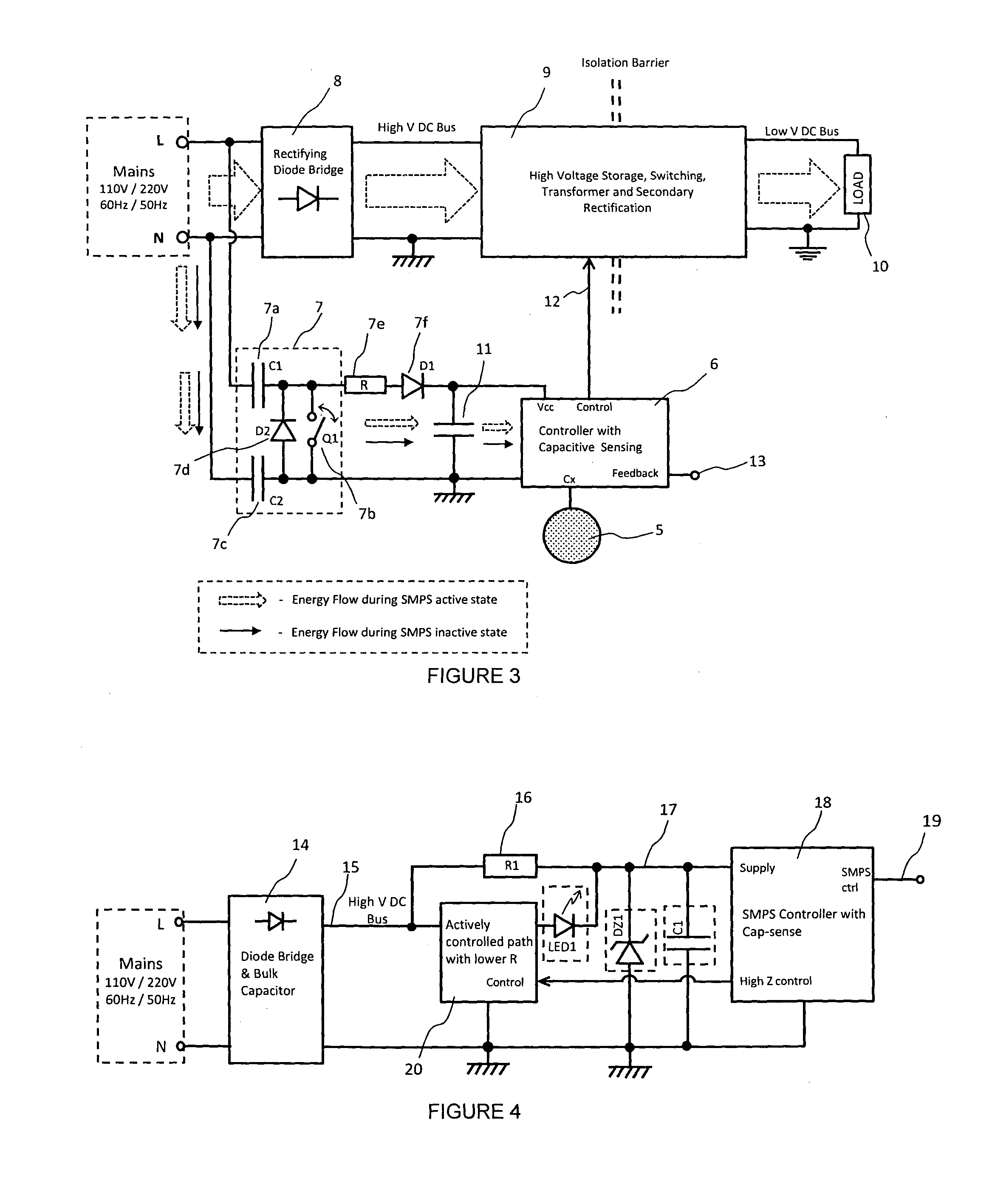
[0017]A microchip may be used for both capacitive sensing and to control the SMPS, according to the present invention. In a first instance, the microchip may be supplied with power via an alternative high impedance energy path distinct from the main energy path through the SMPS. Said high impedance energy path supplying the microchip may for example be resistive, capacitive or inductive in nature, or a combination of the three. The present invention also teaches that more than one rectifying path may be used to minimize losses even further during the inactive state of said switch mode power supply. That is, a first rectifying path may be used to provide power for conversion by the switching section of the SMPS, and consumption by the main load. A second rectifying path is used to provide power to said microchip via a low power, power supply structure, wherein high impedances are placed on the mains side of the diodes in the second rectifying path, thereby causing most of the mains alternating current (AC) voltage to fall across said high impedances. In a preferred embodiment, the high impedances are provided by two capacitors in series with the diodes of said second rectifying path, one connected to the mains live voltage, and the other to the mains neutral voltage, and the mains voltage is sufficiently dropped over these capacitors. These are used to supply said microchip with a so-called cap-dropper supply. A resistor may be placed in series with said capacitors to improve immunity to fast high current surges. The present invention further teaches that a switching element, for example a transistor, may be used to regulate the low voltage direct current (DC) bus, said bus used to supply said microchip. This regulating transistor is effectively used to short-circuit the low AC-voltage present before the diodes of the second rectifying path when said low DC voltage bus is high enough, thereby placing only the series combination of said two capacitors onto the mains AC-voltage, with regards to the second rectifying path. This results in the power being drawn by said second rectifying path when said regulating transistor is closed being mainly reactive. When said regulating transistor is opened, real power drawn by said second rectifying path increases, as the diode or diodes of the path conduct current, and the low DC-voltage bus capacitance is filled. Said controlling microchip may be used to switch the regulating transistor on and off according to the detected state of said low DC-voltage bus. To protect the regulating transistor in its open state from excessive mains related voltages if said second rectifying path utilizes a half-wave diode bridge, a diode may be placed across the low AC-voltage bus, that is across the voltage present after said high impedances, and before said half-wave bridge. This diode across said low AC-voltage bus short-circuits the bus during, for example, the negative mains half cycle, thus protecting the regulating transistor.
[0079]If the frequency at which said blanking pulses repeat is in the audible band, for example if ten blanking pulses are present in each mains half-cycle (that is repetition occurs at 500 Hz), resultant audible emissions may become a nuisance to users. The present invention teaches that such audible emissions may be avoided by increasing the blanking repetition frequency while maintaining the ratio between the period that the main switching element of the SMPS is turned on and the period that it is turned off, taken over the previous blanking repetition period, which will result in the same amount of power transferred. That is, audible emissions may be avoided by applying blanking of said SMPS switching pulses at a higher rate, but with shorter blanking periods, to ensure that the same amount of power than before is transferred. In essence the SMPS switching is spread as evenly as possible over time.

Problems solved by technology

Nonetheless, some losses are still incurred by these efficient switching circuits, which may be anything between a few and multiples of ten percent of the total energy processed and transferred to the load.
However, the SMPS will typically not join this entry into a low power mode, and as such, incur unnecessary losses.
But this action may result in an end device which is not powered anymore and consequently not being able to sense when a user require the system to power up again.
However, such a scheme may require an unnecessarily large low voltage energy store, and could be prone to reliability issues.
An additional challenge is that the power-up sequence needs to be with as little delay as possible.
This results in quite a challenge to keep track of when each mobile device needs to be charged, what charger should be used, and the location of each charger.
The prior art contains a number of solutions to address these problems, for instance as disclosed in U.S. Pat. No. 7,952,320 to Research In Motion, but to date, a simple, robust and cost-effective universal charging solution for portable electronic devices is still not widely available, possible due to lack of robust, low cost communication platforms and power consumption challenges.
However, the underlying premises of the technology is quite old.
However, a number of challenges still hinder deployment in certain areas.
Wireless transceivers tend to be fairly costly components, even in integrated circuit form.
Emissions from wireless transceivers also tend to travel well beyond that which is intended, due to the nature of the technology, opening up to possibility of illegal reception and demodulation, often for criminal purposes.
This necessitates the need for complex encryption of data whenever wireless data transfer is used for secure transactions.
However, a fair amount of energy is required to transfer the energy inductively.
Therefore, the reader can never enter a truly low power state, as it needs to be able to recognize a valid card approach or presence to wake from such a low power state, and this ability requires a fair amount of power.
In capacitive sensing applications, noise may present implementation and utilization challenges, due to the highly sensitive circuits used to sense changes in capacitance.
Specifically common mode noise, or noise currents that flow to the electrical earth, can be detrimental to capacitive sensing systems, given that capacitive sensing electrodes always couple with said earth, be it intentional, as with self-capacitance measurements, or unintentional, as with mutual capacitance measurements.
Especially the lower frequencies of this band coincide with typical charge transfer frequencies used for capacitive sensing, potentially causing problems.
If charge is transferred to and from an unknown capacitor such as a touch electrode at only one frequency, common mode conducted noise at this frequency may disrupt the capacitive sensing process, leading to either the false annunciation of touch or proximity events or an inability to sense real touch or proximity events.
However, the amount of spread that can be realistically realized is limited, both from a hardware perspective, and by sensitivity for human touch, which seems to be optimum at charge transfer frequencies around 500 kHz to 1 MHz.
However, if prior art SMPS controllers are used to power fluorescent or LED based lighting fixtures, the SMPS will have to be active continuously, to power said intelligent user interfaces.
This will inevitably increase power wastage over that of a traditional mechanical switch implementation, negating some of the efficiency gains achieved through the use of LED or fluorescent technology.
In lighting fixtures of the prior art, another drawback is the absolute nature of control, specifically that executed with round knobs traditionally used to dim light sources, or single touch sensor (TS) dimmers.
Further, prior art control knobs suffer from the fact that they are difficult to locate in the dark, as is often the case when a lamp or lighting fixture needs to be turned on.
Single TS dimmers suffer from the drawback that the achieved light level is fixed beforehand according to the time that the TS is engaged.
This can be an inconvenience.
However, said method has the significant drawback that the user has to continuously and rapidly operate said main power switch for a fair number of open / close cycles.
This may not be acceptable, from a user convenience point of view, or from a mains power switch lifetime viewpoint.
In prior art SMPS supplies, audible noise being emitted by a transformer in the supply, due to switching, may be a nuisance to users.
Said noise may also occur in lighting applications where dimming is executed by repetitively keeping the main switching element or elements turned off for one or a number of cycles, reducing the amount of energy transferred by said transformer.

Method used


Image

  • Capacitive sensing enabled switch mode power supply and data transfer
  • Capacitive sensing enabled switch mode power supply and data transfer
  • Capacitive sensing enabled switch mode power supply and data transfer

Examples


Embodiment Construction

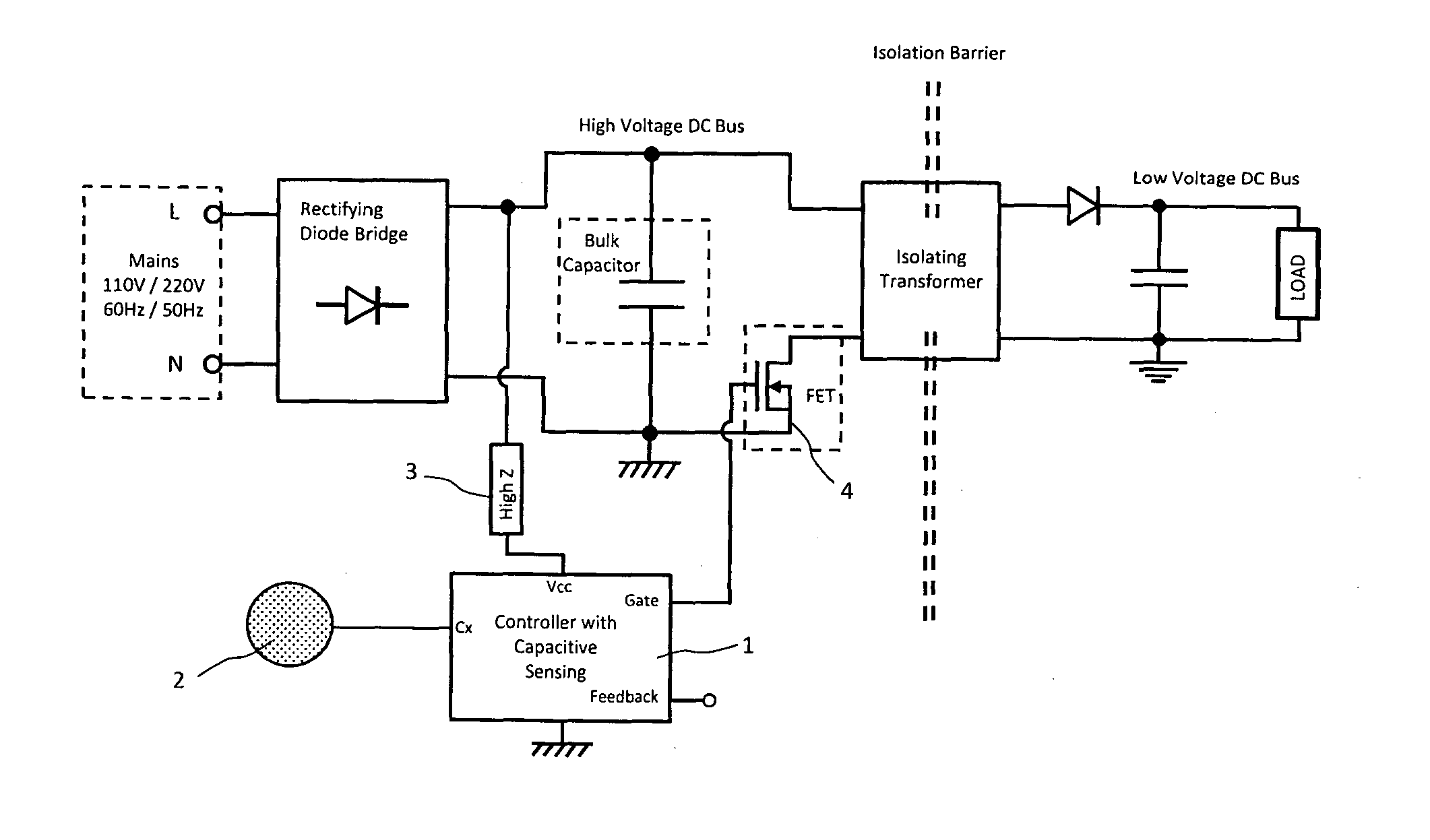
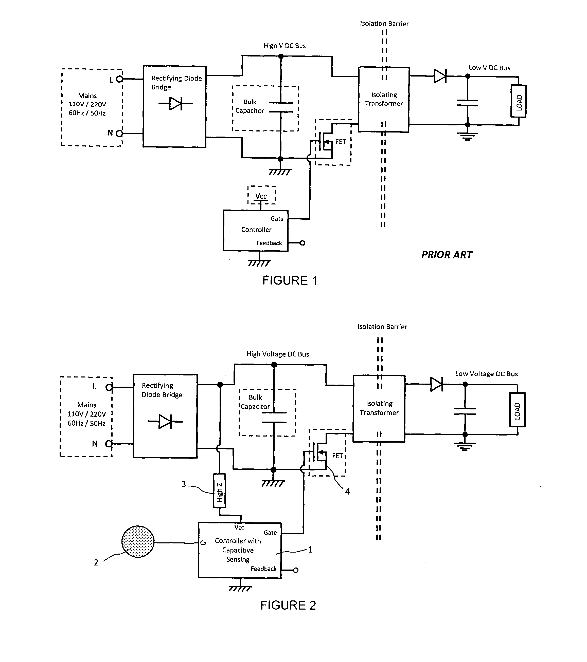
[0112]FIG. 2 shows an exemplary SMPS that applies some of the teachings of the present invention. The alternating current (AC) supply from the mains, or utility network, is typically rectified by a diode bridge, resulting in a high level direct current (DC) voltage. This voltage may typically be maintained by a fairly large bulk capacitor, used as temporary energy store. For a fly-back converter, as illustrated, a main switching element, MOSFET (4) in the example shown, may be closed, which may allow current to build up through the primary winding of an isolation transformer, fed from the bulk capacitor. When said main switching element (4) is opened, the magnetic energy stored in the primary winding of the transformer will typically be commutated to the secondary winding, hence the name fly-back. The voltage at the secondary may depend on the turns ratio of the transformer. After rectification and storage in a secondary bulk capacitor, the output voltage may be fed to the load. In ...


PUM


Abstract

A microchip for control of a switch mode power supply (SMPS), with said microchip also having the ability to measure capacitance of an electrode or sense plate structure or structures, and use of a low power, power supply structure to supply said microchip, said power supply structure distinct from the main energy path via said SMPS to a load. The microchip may control said SMPS to transition between an active state and an inactive state, with the measured capacitance used to determine a condition for state transition. In said SMPS inactive state, only the microchip draws power to operate its capacitive sensing circuitry, leading to a significant SMPS standby losses decrease compared to prior art. Further teachings by the present invention include capacitive sensing based data transfer, universal charging platforms for mobile devices, noise immunity enhancements, various lighting embodiments as well as SMPS operation improvements.

Description

BACKGROUND OF THE INVENTION[0001]The present invention pertains to switch mode power supplies and control thereof, and to the possible use of capacitive sensing to enable and / or improve such control.ii. a) Standby Consumption of Power Electronics:[0002]Power Electronics and switch mode power supplies have become a mature technology, and finds wide application in today's world. It is notable that almost all portable electronic devices contain some sort of Switch Mode Power Supply (SMPS). A typical example is shown in FIG. 1. Due to the fact that a SMPS typically exhibits high efficiency, it is attractive for mobile or portable electronic devices, as these normally run off batteries. Nonetheless, some losses are still incurred by these efficient switching circuits, which may be anything between a few and multiples of ten percent of the total energy processed and transferred to the load.[0003]Mobile devices that employ SMPS often enter a low power mode after a specific period of inacti...

Claims


Application Information

Patent Timeline
Patent Type & Authority Applications(United States)
IPC IPC(8): H02M3/335H05B33/08H05B37/02H02J7/02G01R27/26H02M1/00H05B44/00
CPCH02M3/33507H02J7/025H02J7/022H05B37/02H05B33/0815G01R27/2605H02M1/36Y02B70/10H05B45/3725H02M1/0006H02M1/0032H02M7/05H02J50/10
Inventor BRUWER, FREDERICK JOHANNESVAN WYK, DANIELDOORDUIN, WILLEM ADRIAAN
Owner AZOTEQ PTY LTD
Why Eureka
Try Eureka