Method for detecting probe wear and probe

A technology for detecting probes and probes, applied to measuring devices, instruments, etc., can solve the problems of reduced test energy, long time consumption, difficulty in judging sticky dirt, etc., and achieves the effect of not easy to misjudge

Inactive Publication Date: 2010-06-23
KING YUAN ELECTRONICS
View PDF0 Cites 10 Cited by
  • Summary
  • Abstract
  • Description
  • Claims
  • Application Information

AI Technical Summary

Problems solved by technology

[0007] The purpose of the present invention is to overcome the defects in the existing method for detecting probe wear and provide a new method for detecting probe wear. The technical problem to be solved is to solve the needs of the current method for detecting probe w

Method used


Image

  • Method for detecting probe wear and probe
  • Method for detecting probe wear and probe
  • Method for detecting probe wear and probe

Examples


Embodiment Construction

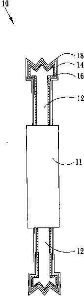
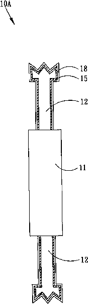
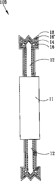
[0034] In order to further explain the technical means and effects of the present invention to achieve the intended purpose of the invention, the method for detecting probe wear according to the present invention and the specific implementation methods and methods of the probe will be described below in conjunction with the accompanying drawings and preferred embodiments. , step, structure, feature and effect thereof, detailed description is as follows.

[0035] Some embodiments of the invention are described in detail below. However, the invention can be broadly practiced in other embodiments than this detailed description. That is to say, the scope of the present invention is not limited by the proposed embodiments, but is subject to the patent scope of the present invention. Secondly, when each element or structure in the illustrations of the embodiments of the present invention is described as a single element or structure, it should not be regarded as a limited cognition...


PUM


Abstract

The invention relates to a method for detecting probe wear and a probe, in particular to a method for online real-time detecting probe wear, the probe and the manufacturing method of the probe. The probe comprises: a probe main body, which comprises at least one needle head; a detecting layer, which coats the needle head or the whole probe main body; and an impact-resistant layer, which is formed on the detecting layer and coats the detecting layer, in order to increase the degree of impact resistance of the probe. The detecting layer with eye-catching color is manufactured inside the probe, which leads the detecting layer of the probe to be exposed after the probe wears, while, the eye-catching color of the probe at the detecting layer serves as a mark, therefore, the online personnel can easily and instantly judge whether the probe wears.

Description

technical field [0001] The invention relates to a method and a probe for detecting wear of a probe, in particular to a method and a probe which are simple, not easy to misjudgment, and can detect the wear of the probe in real time online. Background technique [0002] After the electronic components are manufactured, they usually need to go through circuit probetest, which is used to distinguish the good and bad of the chips before packaging, confirm the quality of the chips for packaging, and avoid the bad quality of the chips caused by packaging. Necessary waste. After packaging, a final test is required to ensure that the chip is not damaged during the packaging process and that the chip still meets the specification after packaging. However, regardless of the above-mentioned tests, the probes are required to be used as electrical connections between the electronic components and the test machine to transmit test signals during the test. [0003] Generally speaking, in ...

Claims


Application Information

Patent Timeline
IPC IPC(8): G01B21/00
Inventor 赵本善陈家进
Owner KING YUAN ELECTRONICS
Why Eureka
Try Eureka