Unlock instant, AI-driven research and patent intelligence for your innovation.

Semiconductor Device Leadless Package Structure

A packaging structure, leadless technology, applied in the direction of semiconductor devices, semiconductor/solid-state device components, electric solid-state devices, etc., can solve the problems of increasing the package size, increasing equipment cost, sensitivity, etc., to reduce the package size, reduce Distance, the effect of reducing product cost

Inactive Publication Date: 2011-12-21
RDA TECH
View PDF0 Cites 0 Cited by
  • Summary
  • Abstract
  • Description
  • Claims
  • Application Information

AI Technical Summary

Problems solved by technology

from figure 1 It can be seen from the figure that since the substrate ground bonding areas 105a, 105b are not adjacent to the circuit die bonding area 102, the ground bonding wires 106a, 106b are longer, because the performance of the power amplifier circuit die is more sensitive to the length of the bonding wire , lengthening the length of the bonding wires 106a, 106b between the connection circuit die bonding regions 107a, 107b and the substrate grounding bonding regions 105a, 105b will affect the overall performance of the device, increase the package size, increase the cost of the device, and ground at the same time The through holes 111a, 111b near the bonding areas 105a, 105b will also increase the package size and increase the equipment cost

Method used


Image

  • Semiconductor Device Leadless Package Structure
  • Semiconductor Device Leadless Package Structure
  • Semiconductor Device Leadless Package Structure

Examples


Embodiment Construction

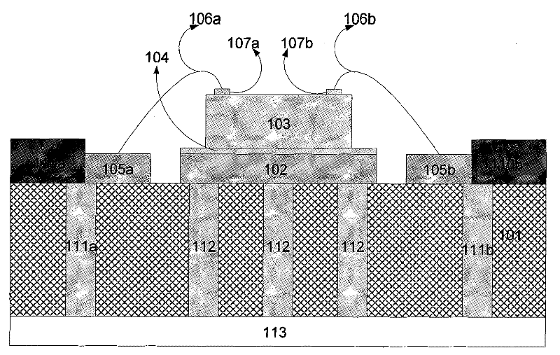
[0017] The invention discloses a leadless packaging structure of a semiconductor device, such as figure 2 and image 3 As shown, it includes substrates 201, 301 and circuit dies 203, 303. The substrates 201, 301 at least include the upper top layer metal, the middle dielectric layer and the lower bottom metal 213, the bottom metal 213 is ground, and the The top layer metal includes circuit die sticking areas 202, 302, the circuit die sticking areas 202, 302 and the circuit dies 203, 303 are bonded together by an adhesive 204, and the circuit die sticking areas A raised first solder resist layer 209a, 209b, 309a, 309b is provided above the edge 214a, 214b, and the top layer metal is provided outside the circuit die attaching area 202, 302 with the circuit die attaching area 202, 302 Electrically connected substrate ground bonding areas 205a, 205b, 305a, 305b, the second solder resist layer 211a, 211b is arranged outside the substrate ground bonding areas 205a, 205b, 305a, 305...


PUM


Abstract

The invention discloses a leadless packaging structure of a semiconductor device, comprising a substrate and a circuit tube core, wherein the substrate at least comprises upper top metal, a middle dielectric layer and a lower bottom metal, wherein the bottom metal is used as the ground; the top metal comprises a circuit tube core pasting area bonded together with the circuit tube core through an adhesive; a raised first solder mask layer is arranged above the edge of the circuit tube core pasting area; the top metal is provided with a substrate grounding and bonding area electrically connected with the circuit tube core pasting area outside the circuit tube core pasting area, and the substrate grounding and bonding area is externally provided with a second solder mask layer; a circuit tube core bonding area on the circuit tube core is connected with the substrate grounding and bonding area through a grounding and bonding wire; the first solder mask layer limits the adhesive in an area within the substrate grounding and bonding area; and the circuit tube core pasting area on the substrate is connected with the bottom metal through a through hole and then grounded. The leadless packaging structure reduces the packaging size of the semiconductor device and reduces the product cost.

Description

technical field [0001] The invention relates to a structure of a semiconductor device, in particular to a leadless packaging structure of a semiconductor device. Background technique [0002] The field of wireless communication is facing the challenges of improving product integration, reducing product size and reducing product cost. The requirements for smaller, more complex and faster products not only challenge the design of circuit dies, but also The fabrication of various package structures presents new challenges. [0003] Bonding wires are often used to form inductance in leadless packages. Bonding wires are very thin metal wires used to connect circuit dies and package pins. The circuit dies are circuit tubes fixed to the substrate by adhesives. core bonding area, and then use the bonding wire to electrically connect the circuit die bonding area to the substrate grounding bonding area. There are usually through holes near the substrate grounding bonding area to conn...

Claims


Application Information

Patent Timeline
Patent Type & Authority Patents(China)
IPC IPC(8): H01L23/488H01L23/58H01L23/498
CPCH01L2924/30107H01L2224/48091H01L24/32H01L2224/73265
Inventor 陈俊谢利刚
Owner RDA TECH