Light-emitting device

A technology of light-emitting components and light-emitting layers, which is applied in the direction of electrical components, light-emitting materials, electroluminescent light sources, etc., can solve the problems of lack of, no brightness and luminous efficiency, insufficient brightness and luminous efficiency, etc. The effect of combining areas and improving luminous efficiency

Inactive Publication Date: 2010-08-18
DAI NIPPON PRINTING CO LTD
View PDF3 Cites 12 Cited by
  • Summary
  • Abstract
  • Description
  • Claims
  • Application Information

AI Technical Summary

Problems solved by technology

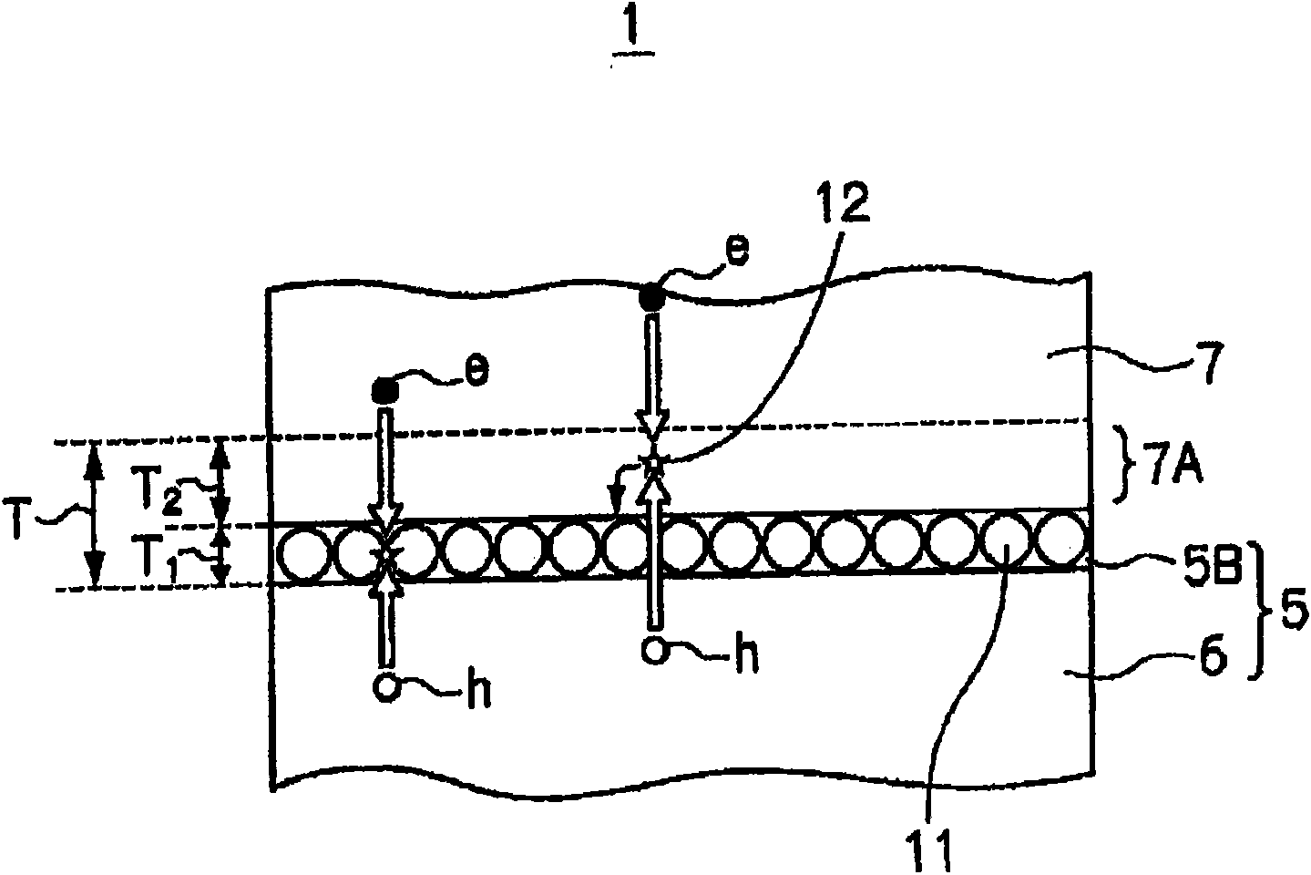
[0006] However, as the literature figure 1 As shown, the light-emitting element proposed in this document has a light-emitting layer that is a monomolecular film of quantum dots, so there is a problem that excitons generated by recombination of charges injected from both electrodes do not reach the monomolecular film. The opportunity to emit light is consumed by EL, and cannot achieve sufficient brightness and luminous efficiency
Furthermore, in this document, an attempt was made to provide a hole blocking layer between the light-emitting layer and the electron transport layer to increase the recombination probability in the light-emitting layer, but it did not bring sufficient brightness and luminous efficiency.

Method used


Image

  • Light-emitting device
  • Light-emitting device
  • Light-emitting device

Examples


Embodiment 1

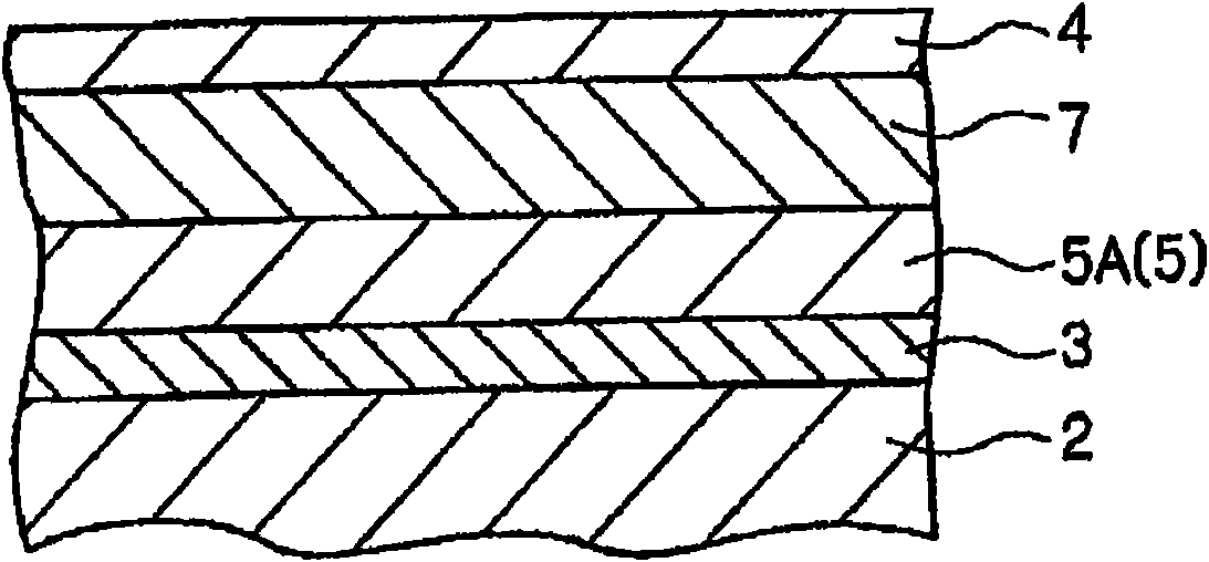
[0087] On a glass substrate, first, a thin film (thickness: 150 nm) of indium tin oxide (ITO) was formed by a sputtering method to form an anode. The substrate on which the anode was formed was cleaned and subjected to UV ozone treatment. Then, in the air, a polyethylenedioxythiophene-polystyrenesulfonate (abbreviation: "PEDOT-PSS") coating solution was applied on the ITO film by spin coating, and dried to form a hollow film. Hole injection layer (thickness: 20 nm).

[0088] Next, N,N-diphenyl-N,N-di( 3-methylphenyl)-1,1-biphenyl-4,4-diamine (TPD) and quantum dots (manufactured by Evident Technologies, core: CdSe, shell: ZnS, emission wavelength: 520nm) mixed with toluene The mixed solution was spin-coated on the hole injection layer to form a hole transport layer and a light emitting layer (total thickness: 40 nm). The hole transport layer and light-emitting layer are separated from the quantum dots of TPD, and the light-emitting layer composed of quantum dots is formed as...

Embodiment 2

[0096] In Example 1, the hole-transporting layer and the light-emitting layer are formed simultaneously by applying a mixed solution of TPD and quantum dots with a mixing ratio of 9:5 on the hole-injecting layer, and then forming a 60nm-thick layer composed of BAlq2. The light-emitting element of Example 2 was produced in the same manner as in Example 1 except that the electron transport layer composed of BAlq2 was replaced with the electron transport layer.

Embodiment 3

[0098] In Example 2, the light-emitting element of Example 3 was produced in the same manner as in Example 2 except that the thickness of the electron transport layer composed of BAlq2 was changed to 40 nm.


PUM

PropertyMeasurementUnit
thicknessaaaaaaaaaa
thicknessaaaaaaaaaa

Abstract

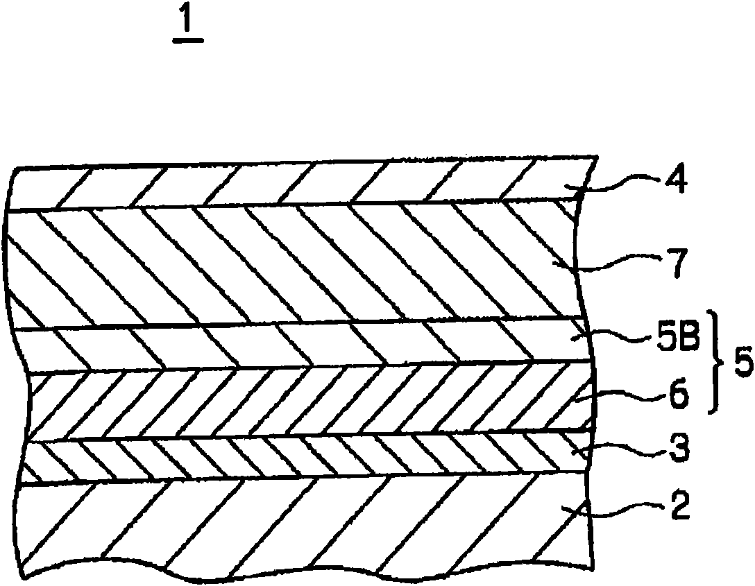
Disclosed is a light-emitting device having a light-emitting layer composed of a monomolecular film of quantum dots, which is enhanced in luminance and luminous efficiency. Specifically disclosed is a light-emitting device (1) comprising at least an anode (3), a hole transporting light-emitting layer (5) composed of a hole transporting material and a quantum dot (11), an electron transporting layer (7) and a cathode (4) in this order. The hole mobility of the electron transporting layer (7) is lower than that of tris(8-quinolinolato)aluminum complex (Alq3), and the hole transporting light-emitting layer (5) is so formed as to emit light when excitons generated in the electron transporting layer (7) are transferred into the light-emitting layer.

Description

[0001] References to related applications [0002] This application is a patent application claiming priority under Article 4 of the Paris Treaty based on Japanese Patent Application No. 2007-256371 (filed on September 28, 2007). Therefore, this application includes all matters disclosed in the patent application specification, drawings, and the like. technical field [0003] The present invention relates to a light-emitting element, and more specifically, to a light-emitting element including an EL light-emitting layer containing quantum dots. Background technique [0004] An organic electroluminescent element (hereinafter referred to as an organic EL element) is a light-emitting element having a laminated structure in which an organic light-emitting layer is sandwiched between an anode and a cathode, and utilizes holes injected from the anode and electrons injected from the cathode. A self-luminous device that emits light due to recombination in the light-emitting layer. ...

Claims


Application Information

Patent Timeline
Patent Type & Authority Applications(China)
IPC IPC(8): H05B33/14C09K11/06H01L51/50
CPCC09K11/623H01L51/5012C09K11/883H05B33/14C09K11/565H05B33/24H01L51/0081B82Y20/00B82Y30/00H10K85/324H10K50/11H10K50/115
Inventor 赤井智纪下河原匡哉
Owner DAI NIPPON PRINTING CO LTD
Why Eureka
Try Eureka