Area light source and display panel

A surface light source and substrate technology, which is used in the manufacture of electrical components, electric solid-state devices, and semiconductor/solid-state devices, etc., can solve the problems of the inability of light to pass through the light output, insufficient light output, etc., so as to reduce the chance of total reflection and increase the light output. Effect

Active Publication Date: 2012-03-28
AU OPTRONICS CORP
View PDF0 Cites 0 Cited by
  • Summary
  • Abstract
  • Description
  • Claims
  • Application Information

AI Technical Summary

Problems solved by technology

[0004] Since both the organic electroluminescence layer and the transparent conductive layer as electrodes are materials with a high refractive index, part of the light emitted when electrons and holes recombine will form a large-angle incident light due to refraction, so in the case of transparent conductive The interface between the layer and the substrate or the interface between the substrate and the air produces total reflection, so that the light cannot pass through, resulting in insufficient light output

Method used


Image

  • Area light source and display panel
  • Area light source and display panel
  • Area light source and display panel

Examples


Embodiment Construction

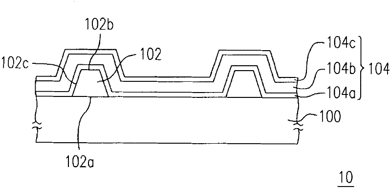
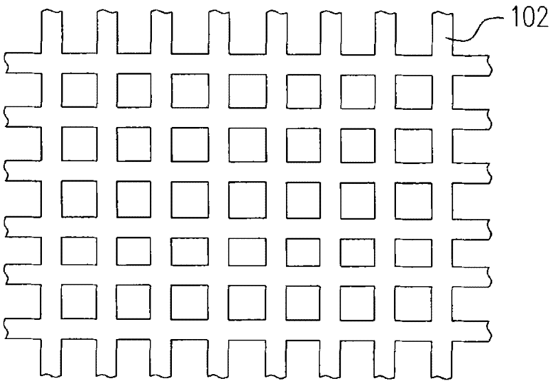
[0046] figure 1 It is a schematic cross-sectional view of a surface light source according to an embodiment of the present invention. Please refer to figure 1 , the surface light source 10 of this embodiment includes a substrate 100 , a patterned scattering layer 102 and an organic electroluminescent element 104 . The substrate 100 is a transparent substrate, such as a glass substrate. The patterned scattering layer 102 is, for example, disposed on a partial area of ​​the substrate 100 . The patterned scattering layer 102 has a bottom surface 102 a in contact with the substrate 100 , a top surface 102 b opposite to the bottom surface 102 a , and a sidewall 102 c connecting the bottom surface 102 a and the top surface 102 b. The included angle between the side wall 102c and the bottom surface 102a is, for example, an acute angle between 5° and 65°. In addition, the area of ​​the top surface 102b is, for example, smaller than the area of ​​the bottom surface 102a. That is, ...


PUM


Abstract

The invention discloses an area light source, which comprises a substrate, a patterned scattering layer and an organic electro-luminescence element, wherein the patterned scattering layer is arranged on a part of the area of the substrate and is provided with a bottom face contacting the substrate, a top face opposite to the bottom face and a plurality of side walls connecting the bottom face andthe top face; and the organic electro-luminescence element is at least arranged on the side walls.

Description

technical field [0001] The present invention relates to a surface light source and a display panel, and in particular to a surface light source and a display panel that can increase the light output of components. Background technique [0002] An organic electroluminescent device is a semiconductor device that can convert electrical energy into light energy and has high conversion efficiency. Its common applications are light-emitting devices for indicator lights, display panels, and optical read-write heads. Because the organic electroluminescent element has characteristics such as no viewing angle problem, simple manufacturing process, low cost, high response speed, wide operating temperature range, and full color, it meets the requirements of display characteristics in the multimedia era and is expected to become the next generation of flat-panel displays. mainstream. [0003] Generally speaking, an organic electroluminescent device includes an anode, an organic light em...

Claims


Application Information

Patent Timeline
Patent Type & Authority Patents(China)
IPC IPC(8): H01L51/52H01L27/32
Inventor 林俊良方俊雄林振祺刘中伟
Owner AU OPTRONICS CORP
Why Eureka
Try Eureka