A light emitting diode and its manufacturing method

A technology of light-emitting diodes and electrodes, which is applied in the direction of electrical components, circuits, semiconductor devices, etc., can solve the problems of limited improvement of LED chip external quantum efficiency, increase of manufacturing cost, increase of process complexity, etc., to improve light extraction efficiency and broad application space , the effect of reducing the probability of total reflection

Active Publication Date: 2017-02-22
XIAMEN CHANGELIGHT CO LTD
View PDF4 Cites 0 Cited by
  • Summary
  • Abstract
  • Description
  • Claims
  • Application Information

AI Technical Summary

Problems solved by technology

Although this technology can improve the external quantum efficiency of the LED chip, there are still the following problems. First, it can only be roughened on one side, and the external quantum efficiency of the LED chip is limited. Second, it is necessary to grow a layer of SiNx protective film, which will increase the cost of the process. complexity, which increases manufacturing costs

Method used


Image

  • A light emitting diode and its manufacturing method
  • A light emitting diode and its manufacturing method

Examples


Embodiment Construction

[0032]The present invention will be described in further detail below in conjunction with the accompanying drawings and specific embodiments.

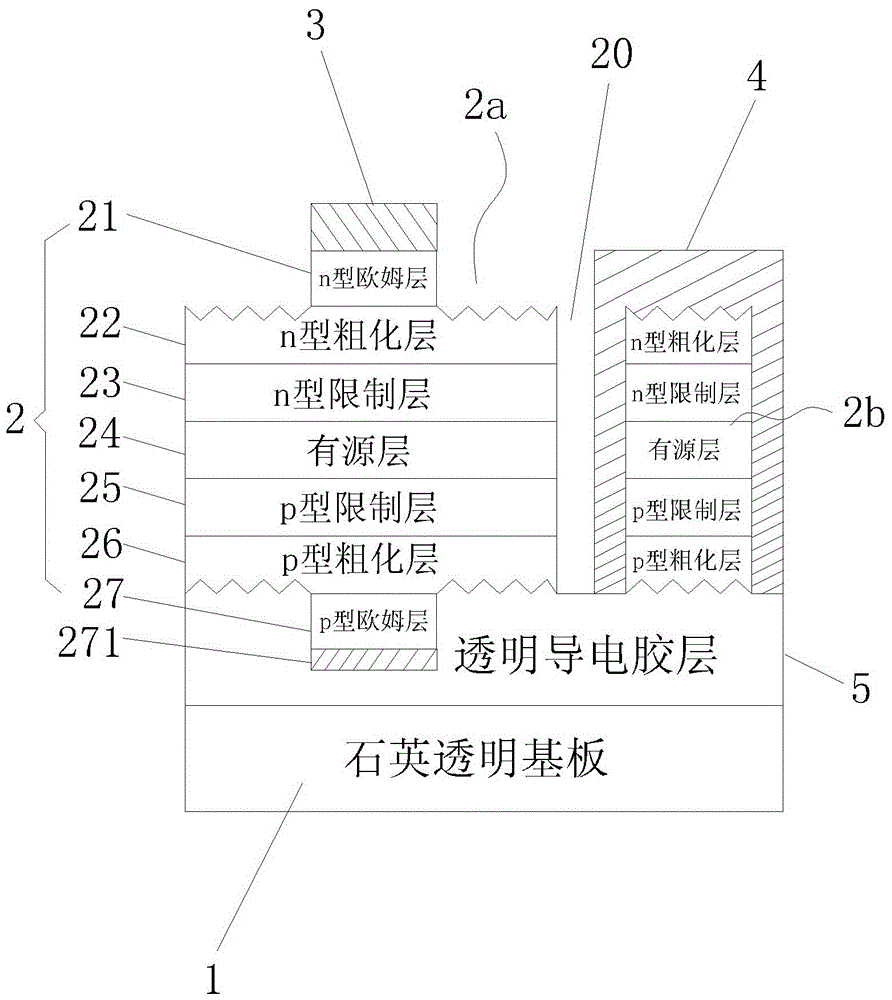
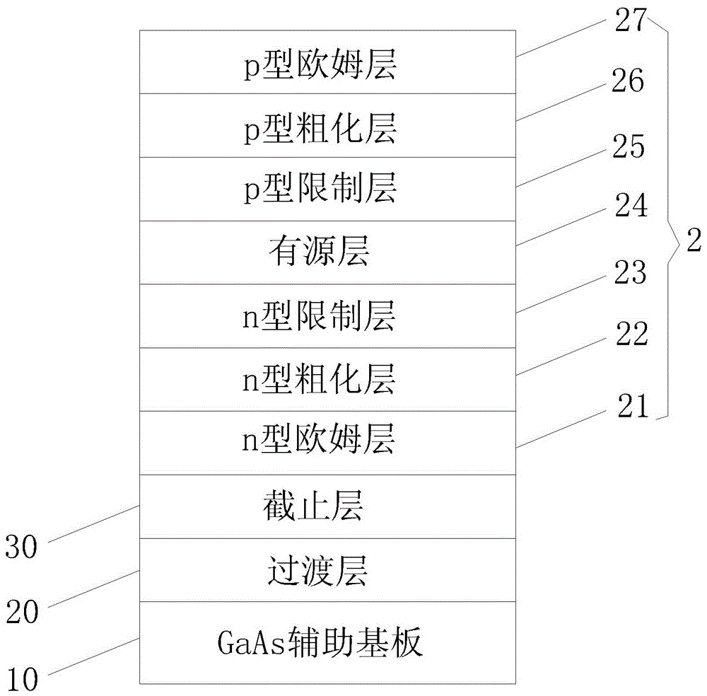
[0033] figure 1 As shown, a light emitting diode includes a transparent substrate 1 made of quartz, an epitaxial wafer 2, a first electrode 3 and a second electrode 4, and the epitaxial wafer 2 sequentially includes an n-type ohmic layer 21, an n-type roughening layer 22. N-type confinement layer 23, active layer 24, p-type confinement layer 25, p-type rough layer 26, p-type ohmic layer 27, the area of ​​the end face of the n-type ohmic layer 21 is smaller than the end face of the n-type rough layer 22 The area of ​​the end face of the p-type ohmic layer 27 is smaller than the area of ​​the end face of the p-type roughened layer 26, the outer end face of the p-type ohmic layer 27 is also plated with an alloy layer 271, and the epitaxial wafer 2 rests on the p-type roughened layer 26 and one side of the p-type ohmic layer 27 are bonded...


PUM


Abstract

The invention discloses a light-emitting diode of a novel structure. The light-emitting diode comprises a transparent substrate, an outwards-extending sheet, a first electrode and a second electrode. The outwards-extending sheet sequentially comprises an n type ohm layer, an n type roughening layer, an n type limiting layer, an active layer, a P type limiting layer, a p type roughening layer and a p type ohm layer. The area of the end face of the n type ohm layer is smaller than that of the end face of the n type roughening layer, the area of the end face of the p type ohm layer is smaller than that of the end face of the p type roughening layer, one side, close to the p type ohm layer and the p type roughening layer, of the outwards-extending sheet is adhered to the transparent substrate through a transparent conductive adhesive layer, the first electrode is connected to the n type ohm layer, the second electrode is connected to the transparent conductive adhesive layer, the outer surfaces of the p type roughening layer and the n type roughening layer are etched to be in the convex-concave shape through corrosive liquid, and the outer end face of the p type ohm layer is further plated with an alloy layer. The invention further discloses a manufacturing method of the light-emitting diode, the light-emitting diode of the novel structure and the manufacturing method of the light-emitting diode effectively reduce loss of emitted light generated by full reflection in the light-emitting diode and improve light-emitting efficiency.

Description

technical field [0001] The invention relates to the structure of a light emitting diode and its manufacturing method. Background technique [0002] In the field of LED chip manufacturing technology, external quantum efficiency is the main technical bottleneck of high-brightness LED chips. The external quantum efficiency of light-emitting diodes depends on their own internal quantum efficiency and release efficiency. The so-called internal quantum efficiency is determined by the material properties of light-emitting diodes. Determined; release efficiency, which means the ratio of light emitted from the inside of the LED to the surrounding air. The release efficiency depends on the loss that occurs when the light leaves the inside of the diode. One of the main reasons for the loss is that the semiconductor material that forms the surface layer of the LED component has a high refractive index. Total reflection occurs, so that the light emitted inside the LED cannot be emitted....

Claims


Application Information

Patent Timeline
Patent Type & Authority Patents(China)
IPC IPC(8): H01L33/22H01L33/00
CPCH01L33/0062H01L33/0093H01L33/22
Inventor 杨凯白继锋林志伟陈凯轩黄尊祥王向武
Owner XIAMEN CHANGELIGHT CO LTD
Why Eureka
Try Eureka