Light-emitting diode chip and manufacturing method thereof

A technology for light-emitting diodes and a manufacturing method, which is applied to semiconductor devices, electrical components, circuits, etc., can solve problems such as limited current expansion, reduced total reflection of light, and inability to emit outward, so as to improve luminous efficiency and brightness, and improve expansion. , the effect of improving brightness

Active Publication Date: 2016-05-18
ANHUI SANAN OPTOELECTRONICS CO LTD
View PDF15 Cites 0 Cited by
  • Summary
  • Abstract
  • Description
  • Claims
  • Application Information

AI Technical Summary

Problems solved by technology

and figure 1 Similarly, the light rays 2a and 2b do not undergo total reflection, and pass through the P-type layer 203 and the current spreading layer 204 to exit; since the upper surface of the P-type layer 203 is roughened, the probability of total reflection of the light is reduced, and the light-emitting layer The emitted light 2d passes through the surface-roughened P-type layer 203 and the current spreading layer 204 and exits outwards; while a part of the light, such as 2d and 2e, still undergoes total reflection and cannot be emitted outwards, thus causing light loss. The improvement of light efficiency has certain limitations. In addition, the current expansion of the above-mentioned current expansion layer structure is relatively limited.

Method used


Image

  • Light-emitting diode chip and manufacturing method thereof
  • Light-emitting diode chip and manufacturing method thereof
  • Light-emitting diode chip and manufacturing method thereof

Examples


Embodiment 1

[0041] A method for manufacturing a light-emitting diode chip, the manufacturing steps comprising:

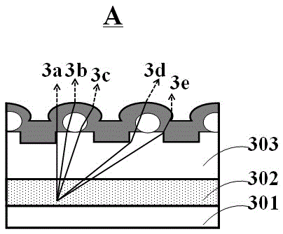
[0042] The first step: if image 3 As shown, a substrate 300 is provided, and the substrate can be an epitaxial substrate, a thermally conductive substrate, a conductive substrate or an insulating substrate. In this embodiment, sapphire (Al 2 o 3 ) as an epitaxial substrate. In other embodiments, the substrate can be a silicon carbide (SiC) substrate, a silicon (Si) substrate, a gallium nitride (GaN) substrate, a gallium arsenide (GaAs) substrate, a gallium phosphide (GaP ) substrates, aluminum nitride (AlN) substrates, copper (Cu) substrates, etc.

[0043] The second step: if Figure 4As shown, metal organic chemical vapor deposition (MOCVD) is used to form an epitaxial layer on the substrate, and the epitaxial layer stacks a first semiconductor layer 301, a light emitting layer 302 and a second semiconductor layer 303 sequentially from bottom to top, wherein the first semi...

Embodiment 2

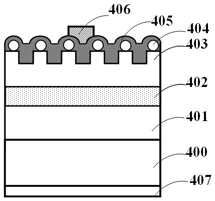
[0051] Such as Figure 11 As shown, different from Embodiment 1, this embodiment discloses a light-emitting diode chip with a vertical structure. In this embodiment, a silicon (Si) substrate is used as the conductive substrate 400, and the N electrode 407 is formed on the back surface of the conductive substrate 400, forming a vertical LED device structure. In addition, the patterned first current spreading layer 404 uses a ZnO nanowire structure, and the cross-sectional diameter of the nanowire is 10-500 nm, preferably 200 nm in this embodiment; the material of the second current spreading layer 405 is a ZnO continuous film, that is Keeping the same refractive index as the patterned first current spreading layer 404, the light path diagram of this embodiment is the same as Figure 10 Similar, and will not be repeated here.

Embodiment 3

[0053] Such as Figure 12 As shown, the difference from Embodiment 2 is that this embodiment uses a copper (Cu) substrate as the conductive substrate 500, and the patterned first current spreading layer 504 uses an ITO nano-column structure. The height of the nano-column is 10-1000 nm, and the width It is 10~10000nm, and in the present embodiment, the height of the preferred nanocolumn is 500nm, and the width is 200nm; The refractive index of the expansion layer, so that the relationship of the refractive index of each material layer is: epitaxial layer > first current spreading layer > second current spreading layer > air, which can further reduce the occurrence probability of total reflection, thereby increasing the light emitting layer. Extraction probability, improve chip brightness and luminous efficiency.

[0054] It should be pointed out that the above-mentioned second current spreading layer 505 material can also be selected from indium tin oxide (ITO), by adjusting I...


PUM


Abstract

The invention discloses a light-emitting diode chip and a manufacturing method thereof. The light-emitting diode chip comprises: an epitaxial layer with a concave-convex microstructure; a patterned first current spreading layer formed on the convex surface of the epitaxial layer; a second current spreading layer Layer, covering the upper surface of the patterned first current spreading layer and the uneven surface of the epitaxial layer without masking the first current spreading layer, the double current spreading layer formed in this way and the epitaxial layer with a concave-convex microstructure can not only Reducing the probability of total reflection and reducing internal reflection and absorption can also improve the expansion of the current, increase the injection efficiency of the current, and reduce the operating voltage of the device, thereby improving the luminous efficiency and brightness of the LED.

Description

technical field [0001] The invention relates to the field of semiconductor devices, in particular to a light emitting diode (LED) chip and a manufacturing method thereof. Background technique [0002] Light-emitting diodes (LEDs) have the advantages of small size, high efficiency and long life, and are widely used in traffic indication, outdoor full-color display and other fields, and have gradually become a research hotspot in the field of electronics. [0003] In order to obtain high-brightness LEDs, the key is to improve the internal and external quantum efficiency of the device. The light extraction efficiency of the chip is the main factor limiting the external quantum efficiency of the device. Due to the large difference in refractive index between the epitaxial material, the substrate material and the air, the light generated by the light-emitting layer is totally reflected at the interface of different refractive index materials and cannot be exported to the chip. ....

Claims


Application Information

Patent Timeline
Patent Type & Authority Patents(China)
IPC IPC(8): H01L33/14H01L33/20H01L33/00
CPCH01L33/20H01L33/42H01L2933/0091
Inventor 郑建森林素慧徐宸科
Owner ANHUI SANAN OPTOELECTRONICS CO LTD
Why Eureka
Try Eureka