Organic light emitting diode display device and organic light emitting diode pixel circuit thereof

A technology of light-emitting diodes and pixel circuits, which can be used in identification devices, static indicators, instruments, etc., and can solve problems such as uneven brightness of the display screen

Active Publication Date: 2010-10-13
AU OPTRONICS CORP
View PDF3 Cites 20 Cited by
  • Summary
  • Abstract
  • Description
  • Claims
  • Application Information

AI Technical Summary

Problems solved by technology

[0007] From the above, it can be seen that the OLED pixel circuit shown in the pixel 148 will cause uneven brightness of the display screen due to th...

Method used


Image

  • Organic light emitting diode display device and organic light emitting diode pixel circuit thereof
  • Organic light emitting diode display device and organic light emitting diode pixel circuit thereof
  • Organic light emitting diode display device and organic light emitting diode pixel circuit thereof

Examples


no. 1 example

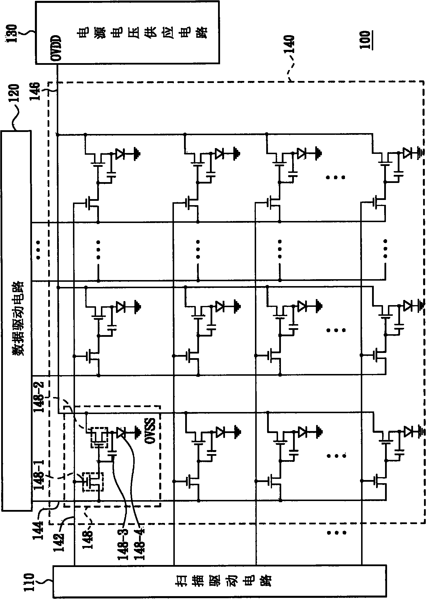
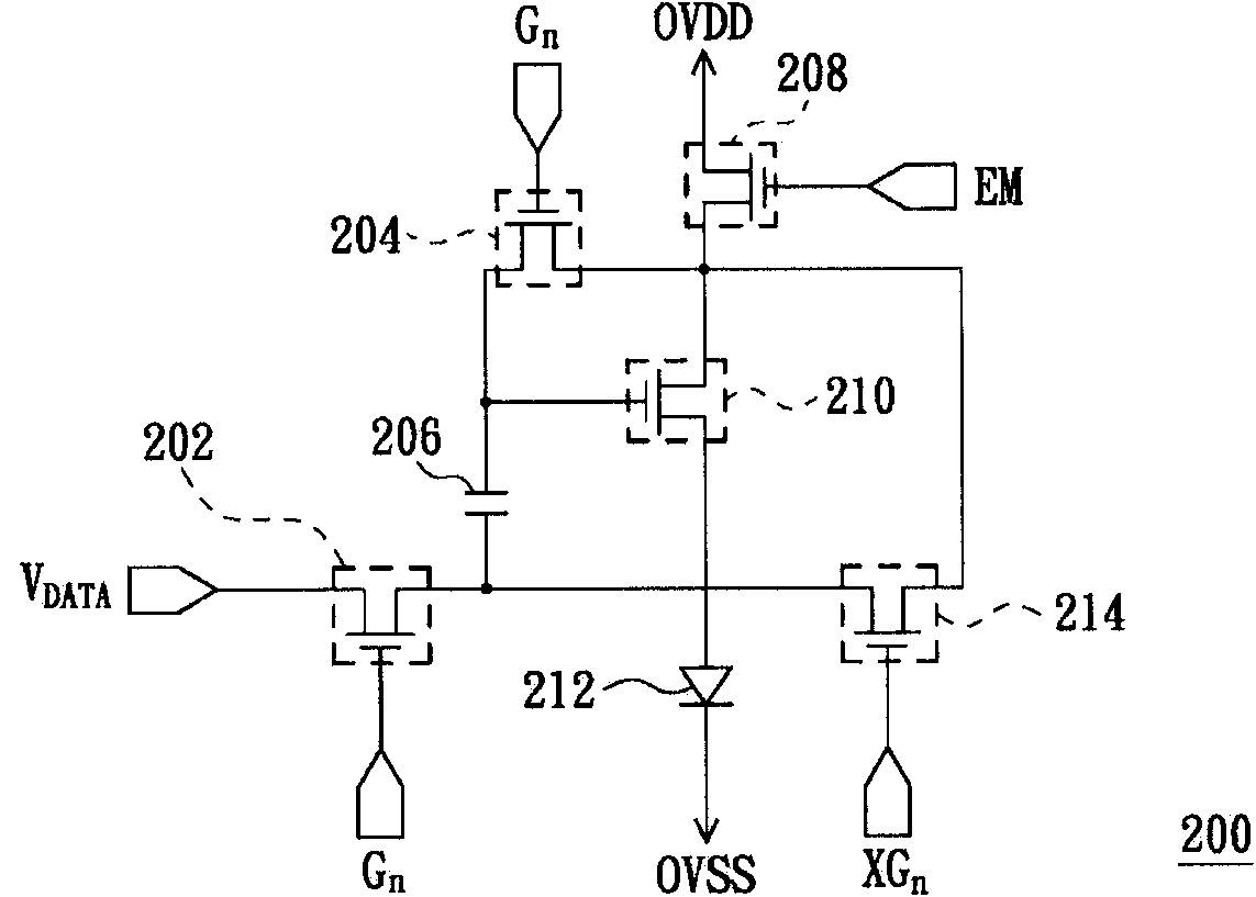
[0053] Please refer to figure 2 , which shows an OLED pixel circuit according to an embodiment of the present invention. The OLED pixel circuit 200 is composed of a transistor 202 , a transistor 204 , a capacitor 206 , a transistor 208 , a transistor 210 (that is, a driving transistor), an OLED 212 and a transistor 214 . In this example, the above five transistors are all realized by an N-type transistor, for example, all are realized by an N-type thin film transistor.

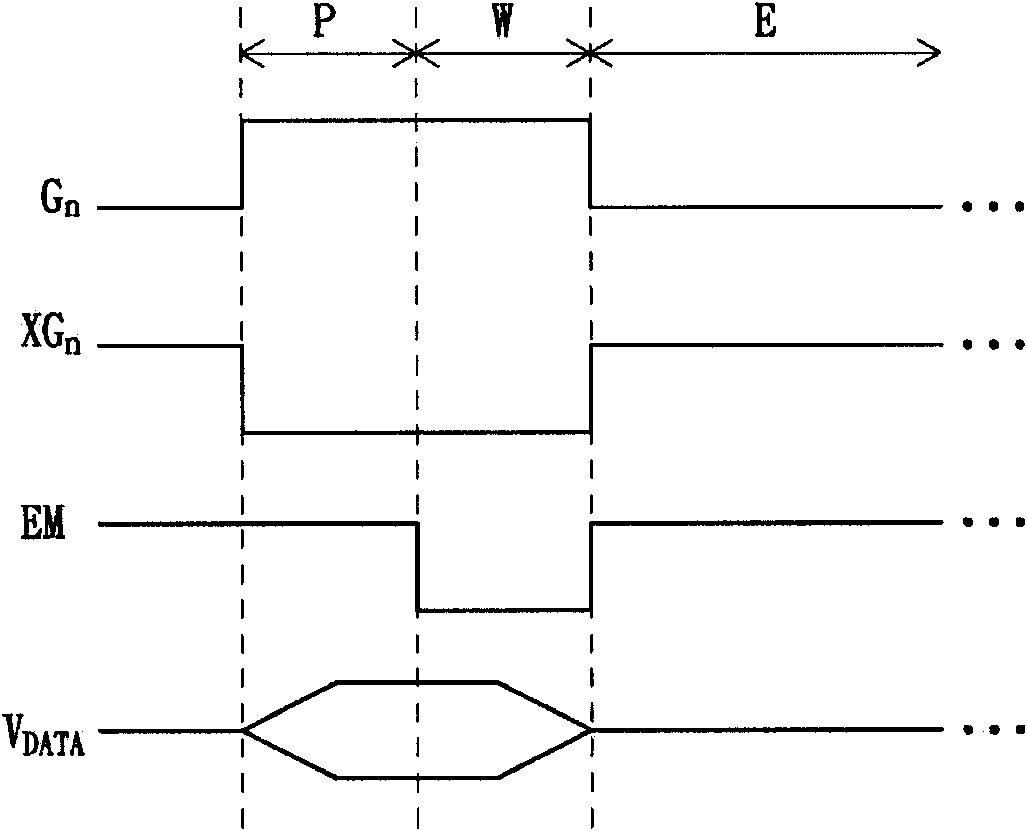
[0054] figure 2 OVDD shown is a power voltage provided by a power voltage supply circuit (not shown). The OVSS shown in the figure is a power supply voltage for reference, such as a ground potential. As a matter of course, the power supply voltage OVDD is greater than the power supply voltage OVSS. In addition, one source / drain of the transistor 202 is suitable for receiving display data V DATA . The gates of the transistors 202 and 204 are both used to receive the scan signal G n , where n is a natur...

no. 2 example

[0078] Through the teaching of the first embodiment, those skilled in the art should know that even if the transistor 214 in the OLED pixel circuit 200 is implemented as a P-type transistor, such as a P-type thin film transistor, The present invention can be realized as Figure 7 shown.

[0079] Figure 7 An OLED pixel circuit according to another embodiment of the present invention is shown. exist Figure 7 In the OLED pixel circuit 700 shown, the transistor 214 has been changed to a P-type transistor, and the gate of the transistor 214 is also coupled to the scan signal G n . while in Figure 7 In the rest of the notation, with the figure 2 The same symbols in represent the same components or signals. The advantage of changing the transistor 214 to a P-type transistor is that the OLED pixel circuit 700 does not need to use the scan signal G n The inverted signal XG n , making the inverted signal XG n can be omitted, and the OLED pixel circuit 700 can still be in a...

no. 3 example

[0081] Through the teaching of the first embodiment, those skilled in the art should know that even if the transistors 202 and 204 in the organic light emitting diode pixel circuit 200 are implemented with a P-type transistor, such as a P-type thin film transistor To realize, also can realize the present invention, as Figure 8 shown.

[0082] Figure 8 An OLED pixel circuit according to another embodiment of the present invention is shown. exist Figure 8 In the OLED pixel circuit 800 shown, both the transistors 202 and 204 have been implemented as P-type transistors, and the gates of the transistors 202 and 204 are also coupled to the scan signal G n The inverted signal XG n . while in Figure 8 In the rest of the notation, with the figure 2 The same symbols in represent the same components or signals. The advantage of changing both the transistors 202 and 204 to a P-type transistor is that the OLED pixel circuit 800 does not need to use the scan signal G n , so th...


PUM


Abstract

The invention relates to an organic light emitting diode display device and an organic light emitting diode pixel circuit thereof. The pixel circuit comprises a first transistor, a second transistor, a third transistor, a fourth transistor, a fifth transistor, a capacitor and an organic light emitting diode, wherein one of source/drain electrodes of the first transistor is suitable for receiving display data, and the other source/drain electrode is coupled with one of source/drain electrodes of the fourth transistor and is coupled with a grid electrode of the second transistor and one of source/drain electrodes of the third transistor through the capacitor; one of source/drain electrodes of the second transistor is coupled with the other source/drain electrodes of the third transistor and the fourth transistor and is coupled with one of source/drain electrodes of the fifth transistor; the other source/drain electrode of the fifth transistor is coupled with a first power supply voltage; the anode and the cathode of the organic light emitting diode are respectively coupled with the other source/drain electrode of the second transistor and a second power supply voltage; and the second power supply voltage is smaller than the first power supply voltage.

Description

technical field [0001] The invention relates to a display technology related to organic light emitting diodes, and in particular to an organic light emitting diode display device and an organic light emitting diode pixel circuit. Background technique [0002] Organic Light Emitting Diode (OLED) panels use organic light emitting diodes as light emitting elements. The organic light emitting diode is a device driven by current, and its luminous brightness will change with the current passing through the organic light emitting diode. Therefore, how to accurately control the current passing through the OLED has become an important issue in the development of the OLED panel. [0003] Please refer to figure 1 , which is a schematic diagram of a conventional OLED display device. The OLED display device 100 includes a scan driving circuit 110 , a data driving circuit 120 , a power supply circuit 130 and a display panel 140 . The display panel 140 further includes a plurality of s...

Claims


Application Information

Patent Timeline
IPC IPC(8): G09G3/32G09F9/33G09G3/3225
Inventor 蔡轩名吴元均
Owner AU OPTRONICS CORP
Why Eureka
Try Eureka