Organic light-emitting diode pixel circuit

A technology of light-emitting diodes and pixel circuits, which is applied to instruments, static indicators, etc., can solve problems such as burn marks on the display screen, lowering the brightness of the organic light-emitting diode 208, and reducing the brightness of the organic light-emitting diode 208.

Active Publication Date: 2010-12-01
AU OPTRONICS CORP
View PDF3 Cites 6 Cited by
  • Summary
  • Abstract
  • Description
  • Claims
  • Application Information

AI Technical Summary

Problems solved by technology

And since the magnitude of the current through transistor 206 is the same as the V of transistor 206 SD voltage is proportional, so the V of transistor 206 SD When the voltage becomes smaller, the current passing through the transistor 206 will also become smaller, further reducing the brightness of the OLED 208
In this way, due to the aging phenomenon of the OLED 208, the brightness of the OLED 208 will be reduced, resulting in burn marks also appearing on the display screen.

Method used


Image

  • Organic light-emitting diode pixel circuit
  • Organic light-emitting diode pixel circuit
  • Organic light-emitting diode pixel circuit

Examples


no. 1 example

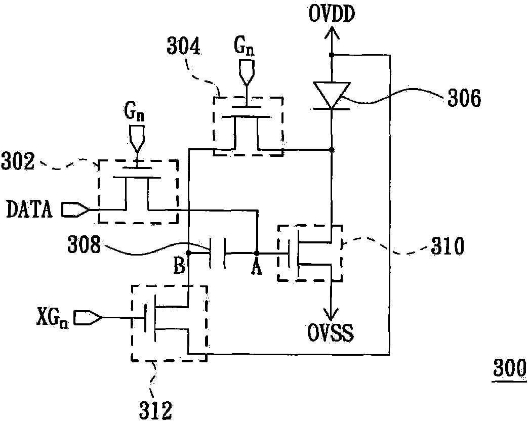
[0049] Please refer to image 3 , which shows an OLED pixel circuit according to an embodiment of the present invention. The OLED pixel circuit 300 is composed of a transistor 302 , a transistor 304 , an OLED 306 , a capacitor 308 , a transistor 310 (ie, a driving transistor) and a transistor 312 . In this example, the above four transistors are all realized by an N-type transistor, for example, all are realized by an N-type thin film transistor.

[0050] image 3 OVDD shown is a power voltage provided by a power voltage supply circuit (not shown). The OVSS shown in the figure is a power supply voltage for reference, such as a ground potential. The power supply voltage OVDD is greater than the power supply voltage OVSS. In addition, one source / drain of the transistor 302 is used to receive the display data DATA. The gates of the transistors 302 and 304 are both used to receive the scan signal G n , where n is a natural number, and G n Indicates the scanning signal trans...

no. 2 example

[0067] Through the teaching of the first embodiment, those skilled in the art should know that even if the transistor 312 in the OLED pixel circuit 300 is not coupled to the power supply voltage OVDD but is instead coupled to a reference voltage, the present invention can also be implemented, as Figure 5 shown.

[0068] Figure 5 An OLED pixel circuit according to another embodiment of the present invention is shown. exist Figure 5 In, marked with image 3 The same symbols in represent the same components or signals. and Figure 5 The OLED pixel circuit 500 shown is also in accordance with Figure 4 The signal timing shown to operate.

[0069] like Figure 5 As shown, the transistor 312 has been changed to couple to a reference voltage V REF . This has the advantage that by changing the reference voltage V REF further changing the size of I OLED The amount of compensation will be further explained below. During the writing period W, the voltage of contact B is as...

no. 3 example

[0076] Through the teaching of the first embodiment, those skilled in the art should know that even if the transistor 312 in the OLED pixel circuit 300 is implemented as a P-type transistor, such as a P-type thin film transistor, it can also Realize the present invention, as Figure 6 shown.

[0077] Figure 6 An OLED pixel circuit according to another embodiment of the present invention is shown. exist Figure 6 In the OLED pixel circuit 600 shown, the transistor 312 has been implemented as a P-type transistor, and the gate of the transistor 312 is also coupled to the scan signal G n . while in Figure 6 In the rest of the notation, with the image 3 The same symbols in represent the same components or signals. The advantage of changing the transistor 312 to a P-type transistor is that the OLED pixel circuit 600 does not need to use the scan signal G n The inverted signal XG n , making the inverted signal XG n can be omitted, and the organic light emitting diode pix...


PUM


Abstract

The invention relates to an organic light-emitting diode pixel circuit. The circuit comprises first to fourth transistors, a capacitor and an organic light-emitting diode, wherein one source / drain of the first transistor receives display data; the grid of a second transistor is coupled with the other source / drain of the first transistor and coupled with one source / drain of a third transistor and one source / drain of a fourth transistor through the capacitor; one source / drain of the second transistor is coupled with a first power supply voltage; the other source / drain of the third transistor iscoupled with the other source / drain of the second transistor; the other source / drain of the fourth transistor receives a reference signal; and the anode and cathode of the organic light-emitting diode are coupled with a second power supply voltage and the other source / drain of the second transistor respectively, wherein the second power supply voltage is more than the first power supply voltage.

Description

technical field [0001] The present invention relates to an organic light emitting diode display technology, and in particular to an organic light emitting diode pixel circuit. Background technique [0002] Organic Light Emitting Diode (OLED) displays use organic light emitting diodes as display elements. The organic light emitting diode is a device driven by current, and its luminous brightness will change with the current passing through the organic light emitting diode. Therefore, how to accurately control the current passing through the OLED has become an important issue in the development of the OLED panel. [0003] Please refer to figure 1 , which is a schematic diagram of a known OLED display. The OLED display 100 includes a scan driving circuit 110 , a data driving circuit 120 , a power voltage supply circuit 130 and an OLED display panel 140 . The OLED display panel 140 further includes a plurality of scan lines (as indicated by 142 ), a plurality of data lines (...

Claims


Application Information

Patent Timeline
Patent Type & Authority Applications(China)
IPC IPC(8): G09G3/32G09G3/3225
Inventor 蔡宗廷吴元均
Owner AU OPTRONICS CORP
Why Eureka
Try Eureka