Systems and methods for link processing with ultrafast and nanosecond laser pulses

A laser pulse and laser system technology, applied in the field of laser processing, can solve the problems of small processing critical difference and failure to reach the processing window

Inactive Publication Date: 2010-11-03
ELECTRO SCI IND INC
View PDF3 Cites 1 Cited by
  • Summary
  • Abstract
  • Description
  • Claims
  • Application Information

AI Technical Summary

Problems solved by technology

These techniques may apply a single ultrafast laser pulse or multiple ultrafast laser pulses at high repetition rates and / or in bursts
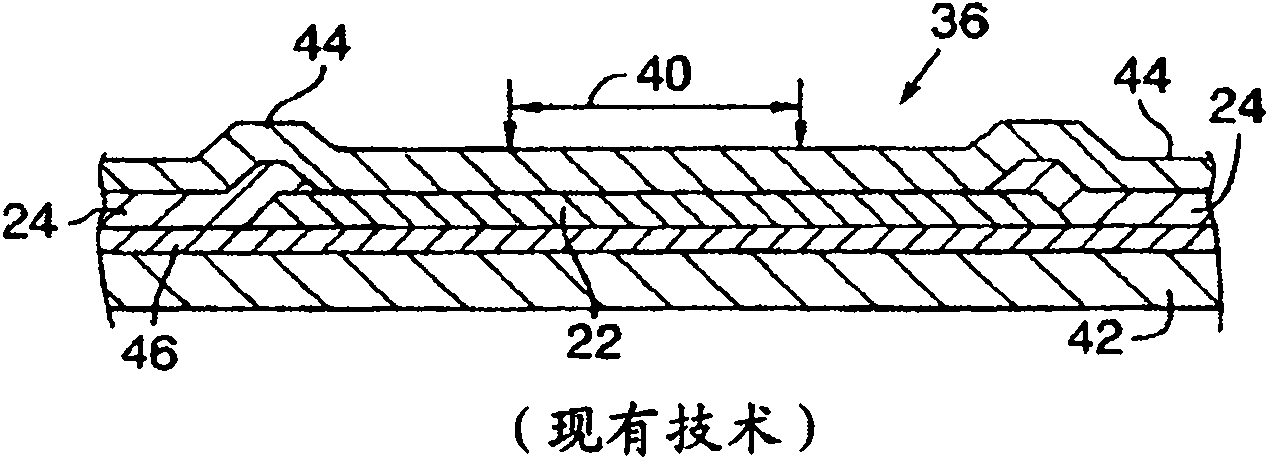
However, while these ultrafast laser pulses are sufficient to remove the upper passivation layer 44 as well as the link 22, there is a critical difference in processing between the material of the link 22 and the material of the lower passivation layer 46 based on laser intensity induced collapse. However, it is too small to achieve a wide process window within which the ultrafast laser pulse can remove all of the bond material without causing any ablation into the underlying passivation layer 46.

Method used


Image

  • Systems and methods for link processing with ultrafast and nanosecond laser pulses
  • Systems and methods for link processing with ultrafast and nanosecond laser pulses
  • Systems and methods for link processing with ultrafast and nanosecond laser pulses

Examples


Embodiment Construction

[0020] The present invention describes the use of an ultrafast laser pulse, or a cluster of ultrafast laser pulses, followed by one or more nanosecond laser pulses to process conductive connections in integrated circuits (ICs), which laser pulses have the conventional temporal pulse shape or custom-made time pulse shape.

[0021] The ultrafast laser pulse or pulses process a passivation material overlying the link and a portion of the link material. In one such embodiment, the ultrafast laser pulse or pulses treat the overlying passivation layer based at least in part on laser intensity induced collapse. In an embodiment, the ultrafast laser pulse or pulses treat a substantial portion of the link.

[0022] Next, a nanosecond laser pulse completes the removal of the remaining bonding material. Since the treatment provided by the nanosecond laser pulse is primarily based on heat generated by laser absorption of the target material and the underlying passivation material is a n...


PUM

PropertyMeasurementUnit
wavelengthaaaaaaaaaa

Abstract

Systems and methods for processing an electrically conductive link in an integrated circuit use a series of laser pulses having different pulse widths to remove different portions of a target structure without substantially damaging a material underlying the electrically conductive link. In one embodiment, an ultrafast laser pulse or bundle of ultrafast laser pulses removes an overlying passivation layer in a target area and a first portion of link material. Then, a nanosecond laser pulse removes a second portion of the link material to sever an electrical connection between two nodes in the integrated circuit. The nanosecond laser pulse is configured to reduce or eliminate damage to the underlying material.

Description

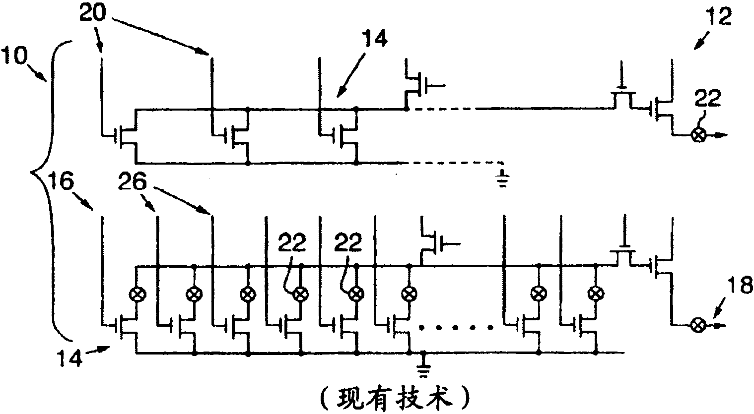
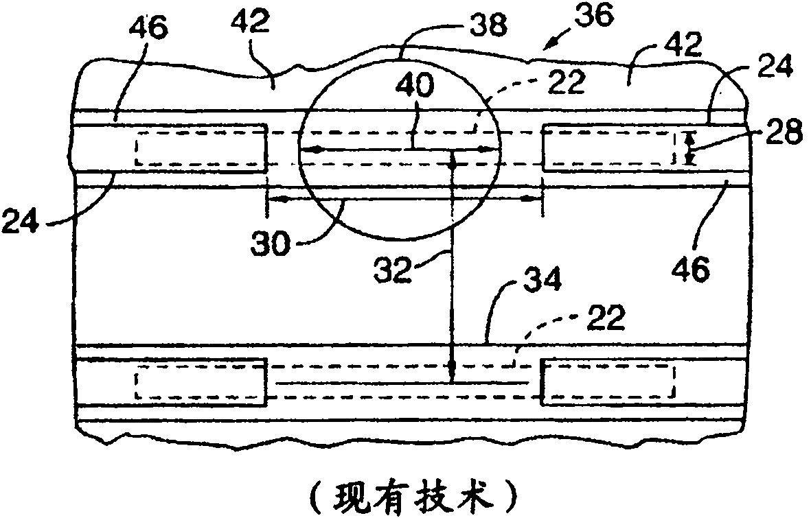
technical field [0001] This invention relates to laser processing of conductive connections in memory or other integrated circuits (ICs). In particular, the present invention relates to systems and methods for cutting conductive links and removing passivation material on those links using ultrafast and nanosecond laser pulses. Background technique [0002] Yields during IC device fabrication often result in defects in relation to variations in the arrangement of sub-surface layers or patterns of particulate contamination. figure 1 , 2A And shown in 2B are individual electronic circuits 10 of an IC device or work piece 12, which are typically fabricated in multiple columns or rows to include multiple repeating redundant circuit components 14, such as spare columns of memory cells 20 16 and alternate row 18. The circuits 10 are also designed to include special laser-cuttable conductive links 22 between electrical contacts 24, for example, they can be removed to disconnect a...

Claims


Application Information

Patent Timeline
Patent Type & Authority Applications(China)
IPC IPC(8): H01S3/10H01L21/302
CPCB23K26/0635H01L23/5258B23K26/0624H01L2924/0002H01L2924/00
Inventor 孙云龙理查·S.·哈洛斯
Owner ELECTRO SCI IND INC
Why Eureka
Try Eureka