

Double-layer crucible for growing silicon single crystals by directional solidification method
A double-layer crucible and silicon single crystal technology, applied in self-solidification, crystal growth, single crystal growth, etc., can solve problems such as leakage of silicon melt, achieve improved performance, easy processing, and avoid dislocation effects
- Summary
- Abstract
- Description
- Claims
- Application Information
AI Technical Summary
Problems solved by technology
Method used
Image

Examples
Embodiment 1
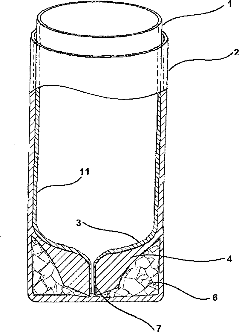
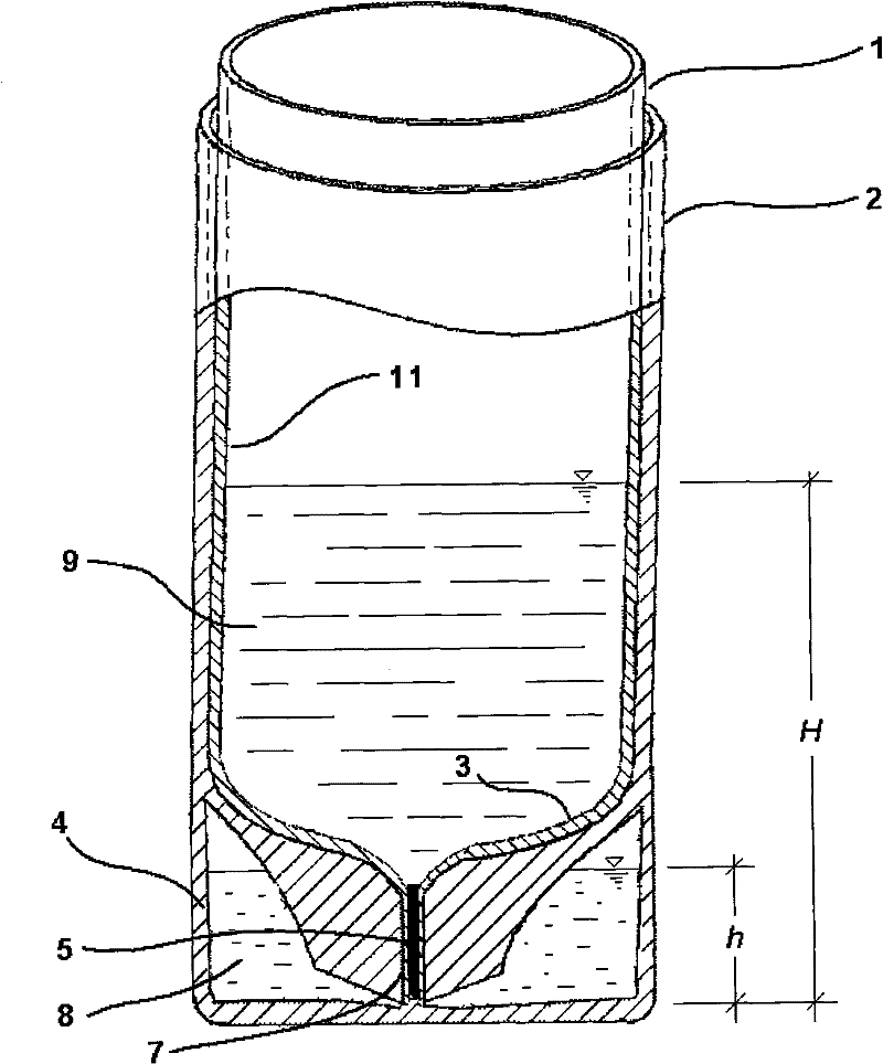
[0036] Such as figure 2 The shown double-layer crucible for growing silicon single crystal by directional solidification method includes an outer crucible and an inner crucible, and the inner crucible is nested inside the outer crucible.
[0037] Wherein, the outer crucible is made of CFC (carbon-carbon composite) material, including the outer crucible main body 2 and the outer crucible bottom 4, and is processed between the inner and outer walls of the outer crucible bottom 4 for placing an anti-leakage agent 6 leak-proof cavity. Anti-leakage agent 6 adopts high-purity tin, and its purity is more than 99.99%. The anti-leakage agent 6 is in a liquid state when the temperature is greater than 232°C, and its density is about 7.3g / cm3, and it does not react with silicon and is immiscible even at high temperatures (1000-2000°C).
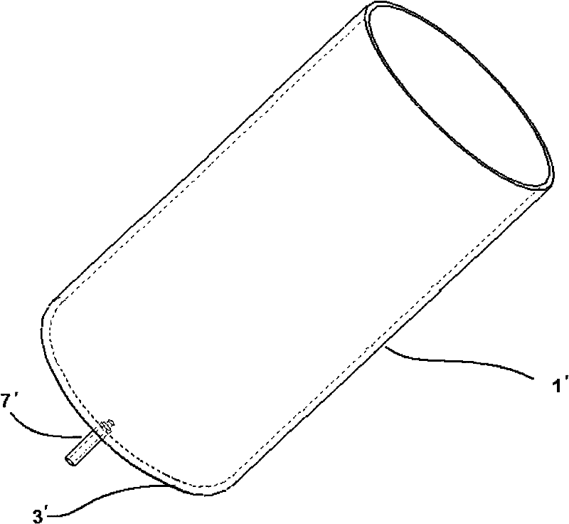
[0038] The inner crucible is made of quartz material, including a quartz inner crucible main body 1, a quartz seed crystal sleeve 7, and a quartz inn...
Embodiment 2
[0045] In the same manner as in Example 1, the difference is that the mass ratio is 1:1 of BaF 2 and BaCl 2 Mixture (powder state) as anti-leakage agent 6. BaF 2 The melting point is 1360°C and the density is 4.89g / cm 3 . BaCl 2 The melting point is 962°C and the density is 3.1g / cm 3 . Therefore, BaF with a mass ratio of 1:1 was used 2 and BaCl 2 The density of the mixture is greater than that of silicon (2.33g / cm3), and the melting point is lower than that of silicon (1415°C). At the same time, BaF 2 and BaCl 2 The melt temperature is between 1400°C and 2000°C, and it does not react with or dissolve in the silicon melt.
Embodiment 3
[0047] The same method as in Example 1 is adopted, except that the cross-sectional areas of the main body 1 of the inner crucible and the main body 2 of the outer crucible are square.
PUM
| Property | Measurement | Unit |
|---|---|---|
| height | aaaaa | aaaaa |
| height | aaaaa | aaaaa |
| melting point | aaaaa | aaaaa |
Abstract
Description
Claims
Application Information