Stacking structure of semiconductor packages

A package and semiconductor technology, applied in the direction of semiconductor devices, semiconductor/solid-state device components, electric solid-state devices, etc., can solve the problems of increasing the cost of assembly materials, increasing the yield rate, and unfavorable overall stacking height

Inactive Publication Date: 2010-11-17
ASE ASSEMBLY & TEST SHANGHAI
View PDF0 Cites 12 Cited by
  • Summary
  • Abstract
  • Description
  • Claims
  • Application Information

AI Technical Summary

Problems solved by technology

Although the combined structure of stacked packages on the existing package can achieve the effect of high-density packaging, it is not conducive to reducing the overall stacking height after stacking and assembly, that is, it cannot provide the advantage of miniaturization, which is not conducive to application in mobile phones, etc. The field of miniaturized electronics
Furthermore, the use of the transit circuit board 13 will relatively increase the cost of assembly materials when stacking.
In addition, during assembly, the first and second transfer metal balls 131, 132 must be assembled twice with the first and second packages 11, 12 respectively, which relatively increases the time required for assembly. and complexity, and will increase the risk of yield decline due to assembly alignment failure

Method used


Image

  • Stacking structure of semiconductor packages
  • Stacking structure of semiconductor packages
  • Stacking structure of semiconductor packages

Examples


Embodiment Construction

[0025] In order to make the above-mentioned purposes, features and advantages of the present invention more obvious and understandable, the preferred embodiments of the present invention will be specifically cited below, together with the accompanying drawings, for a detailed description as follows:

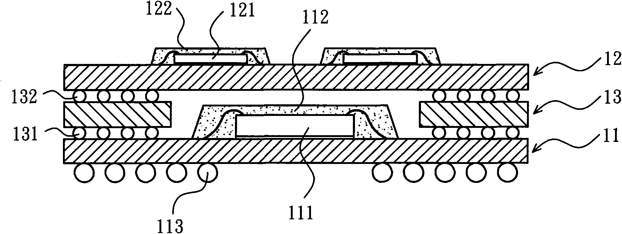
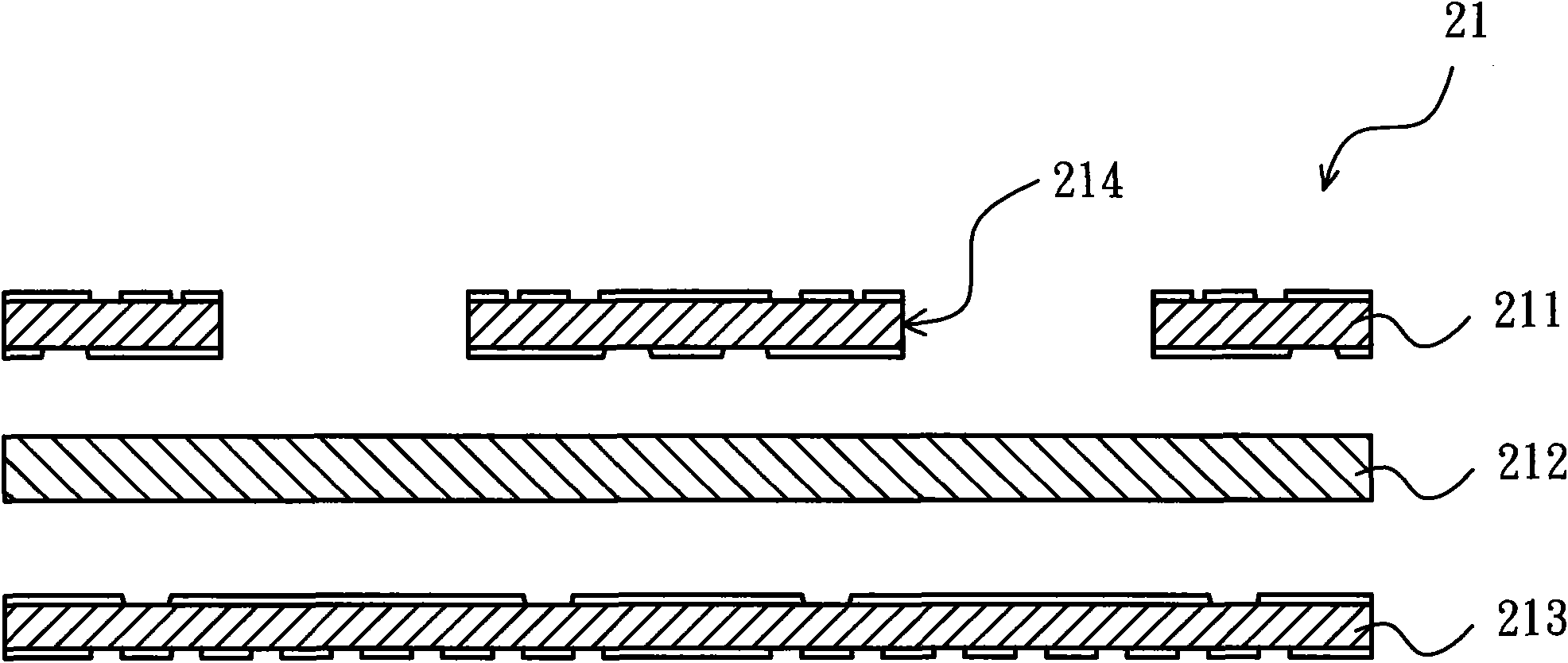
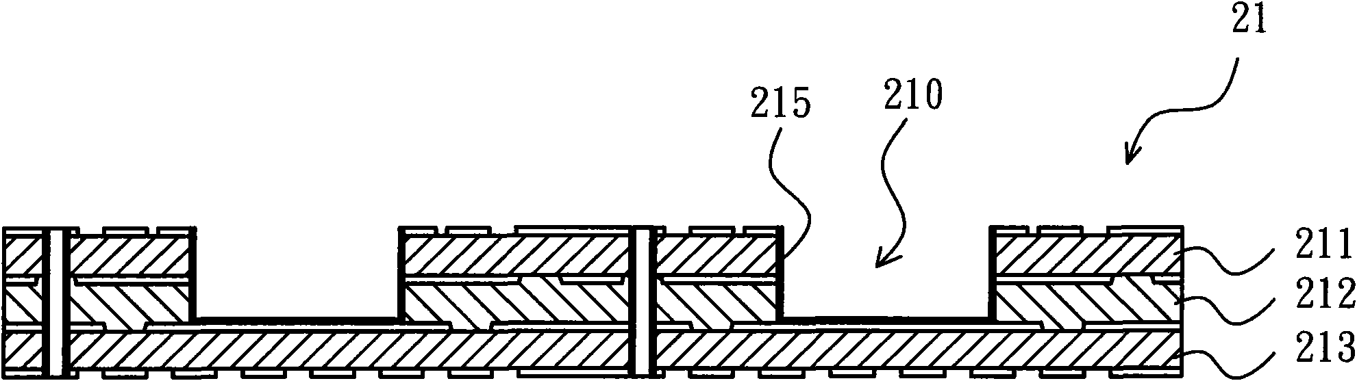
[0026] Please refer to Figure 2A , 2B , 2C, 2D, 2E and 2F, which disclose the manufacturing method flow of the stacked structure of the semiconductor package according to the first embodiment of the present invention, wherein as Figure 2A , 2B As shown in and 2C, the first step of the manufacturing method is: providing a first circuit board 21 provided with at least one cavity 210 and several transfer pads 218 . In this step, if Figure 2A As shown, first, a plurality of substrate units are combined by a lamination process, for example, a first substrate unit 211, a second substrate unit 212 and a third substrate unit 213 are combined, wherein the first substrate unit 211 is...


PUM


Abstract

The invention discloses a stacking structure of semiconductor packages, which comprises a first package, a second package and a plurality of switching elements. The first package is provided with a first circuit board, at least one first chip and at least one first package colloid. The first circuit board is provided at least one depression and a plurality of switching solder pads, the depression accommodates the first chip, and the first package colloid fills the depression and covers the first chip. The switching solder pads are formed on the upper surface of the first circuit board where no depression is arranged. The lower surface of the second package is electrically connected with the switching solder pad of the first circuit board of the first package through the switching element. Because the depression accommodates the chip, the protrusion height caused by the chip and the package colloid can be reduced, and the overall stacking height during stacking assembly can be further reduced.

Description

【Technical field】 [0001] The present invention relates to a stacking structure of semiconductor packages, in particular to a stacking structure of semiconductor packages that can effectively reduce the overall stacking height. 【Background technique】 [0002] Nowadays, in order to meet various high-density packaging requirements, the semiconductor packaging industry has gradually developed various types of packaging structures, among which various system in package (SIP) design concepts are often used to build high-density packaging structures. Generally speaking, system packaging can be divided into multi chip module (MCM), package on package (POP) and package in package (PIP). The multi-chip module (MCM) refers to arranging several chips on the same substrate. After setting the chips, the same packaging gel is used to embed all the chips, and according to the arrangement of the chips, it can be subdivided into stacked chips (stacked chips). die) package or parallel chip (s...

Claims


Application Information

Patent Timeline
Patent Type & Authority Applications(China)
IPC IPC(8): H01L25/00H01L23/13H01L23/488H01L23/48H01L23/34
CPCH01L2924/15311H01L2224/16227H01L2224/73265H01L2224/16225H01L2224/48227H01L2924/3025
Inventor 许宏达叶昶麟赵健
Owner ASE ASSEMBLY & TEST SHANGHAI
Why Eureka
Try Eureka