Supercharge Your Innovation With Domain-Expert AI Agents!

Photonic interconnects for computer system devices

A computer system, photonic technology, applied in the field of photonic interconnection, can solve the problems of energy cost limiting bandwidth, slow growth and so on

Active Publication Date: 2010-12-08
HEWLETT-PACKARD ENTERPRISE DEV LP
View PDF0 Cites 5 Cited by
  • Summary
  • Abstract
  • Description
  • Claims
  • Application Information

AI Technical Summary

Problems solved by technology

Computational bandwidth scales linearly with the number of cores, but the rate at which data can be sent across a multicore chip using top-level metal wires is improving at a much slower rate
In addition, the rate at which data can be transferred off-chip via pins located along the edge of the chip also grows more slowly than computational bandwidth, and the energy costs of on-chip and off-chip communication significantly limit the available bandwidth

Method used


Image

  • Photonic interconnects for computer system devices
  • Photonic interconnects for computer system devices
  • Photonic interconnects for computer system devices

Examples


Embodiment Construction

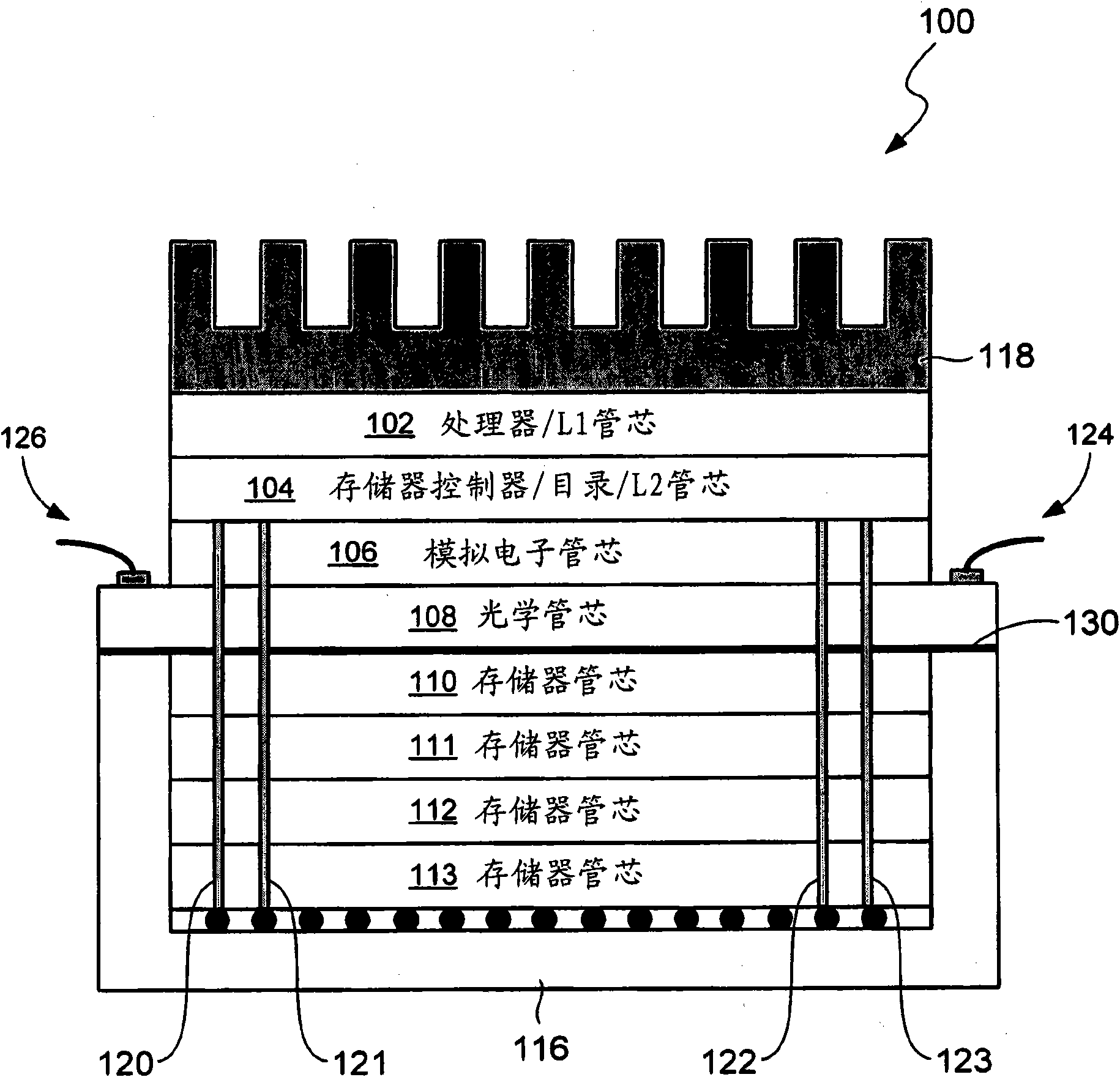
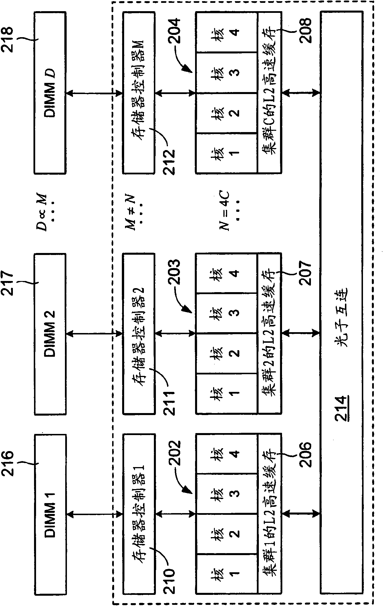
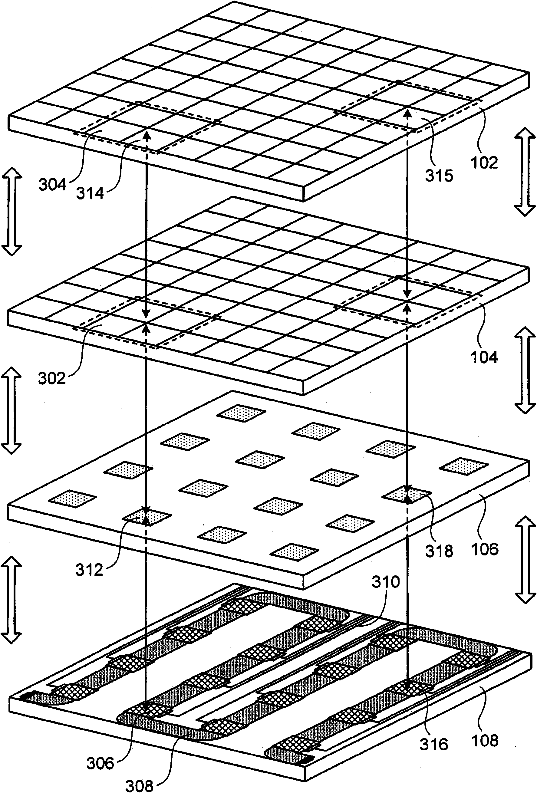
[0030] Various embodiments of the invention relate to photonic interconnects. These photonic interconnects provide on-chip photonic interconnections between computer system components (eg, cores, clusters, memory controllers). In addition, some embodiments of the photonic interconnection also provide off-chip photonic interconnection to computer system components on external devices. Embodiments of the invention also include photonic interconnects having nanophotonic components, including components having dimensions typically smaller than a wavelength or smaller than a micron.

[0031] These photonic interconnects provide data transfer rates off-chip faster than conventional pins located along the edge of the chip, provide greater computing bandwidth, and provide lower on-chip and off-chip communication than conventional metal lines energy costs and can be scaled up or down to accommodate additional components, such as processors with any number of cores. The architecture o...


PUM


Abstract

Various embodiments of the present invention are directed to photonic interconnects that can be used for on-chip as well as off-chip communications between computer system components. In one embodiment of the present invention, a photonic interconnect (108) comprises a plurality of on-chip waveguides (308). Additionally, the photonic interconnect may include a plurality of off-chip waveguides (310,620), and at least one optoelectronic converter (306). The at least one optoelectronic converter (306) can be photonically coupled to a portion of the plurality of on-chip waveguides (308), can be photonically coupled to a portion of the plurality of off-chip waveguides (310,620), and is in electronic communication with at least one computer system component (615-618).

Description

technical field [0001] Embodiments of the invention relate to photonic interconnects that can be used for on-chip as well as off-chip communication between computer system components in computer system devices. Background technique [0002] In the mid-1960's, semiconductor manufacturers observed that the density of circuits (such as transistors) fabricated on integrated circuits doubled approximately every 18 months. This trend has continued and is now known as "Moore's Law". Transistor density is viewed as a rough measure of computer processing power, which in turn corresponds to data processing speed. Although originally derived as an observation, Moore's Law has over time become widely accepted by the semiconductor industry as the fundamental driving force behind increased computer processing power. As a result, semiconductor manufacturers have developed techniques for reducing the size of chip components to microscale and even nanoscale dimensions. Computer system arc...

Claims


Application Information

Patent Timeline
IPC IPC(8): G02B6/12
CPCH04B10/801G02B6/43
Inventor R·G·博索莱尔M·菲奥伦蒂诺N·P·茹皮N·L·宾克特R·S·施雷伯Q·徐
Owner HEWLETT-PACKARD ENTERPRISE DEV LP
Features
  • R&D
  • Intellectual Property
  • Life Sciences
  • Materials
  • Tech Scout
  • Unparalleled Data Quality
  • Higher Quality Content
  • 60% Fewer Hallucinations
Learn More